Zero-power sampling SAR ADC circuit and method

Active Publication Date: 2012-11-08
TEXAS INSTR INC
View PDF7 Cites 45 Cited by
  • Summary
  • Abstract
  • Description
  • Claims
  • Application Information

AI Technical Summary

Benefits of technology

[0039]In one embodiment, the invention provides a switched-capacitor circuit (10, 32 or 32A) for converting a difference between a first input signal (VIN+) and a second input signal (VIN−) to a digital signal (DOUT) so as to prevent leakage of sampled input charge through an integrated circuit substrate diode (25), including means (21 in FIG. 1A and 16 in FIG. 2 or 33 in FIG. 9) for sampling the first input signal (VIN+) onto a first capacitor (C1 or CIN1) by switching a first terminal (top plate) of the first capacitor (C1 or CIN1) through a first conductor (13) to a first reference voltage (VSS), and switching a second terminal (bottom plate) of the first capacitor (C1 or CIN1) to the first input signal (VIN+); means (21 in FIG. 1A and 16 in FIG. 2 or 33 in FIG. 9) for sampling the second input signal (VIN−) onto a second capacitor (C3 or CIN3) by switching a first terminal (top plate) of the second capacitor (C3 or CIN3) to the second input signal (VIN−) and switching a second terminal (

Problems solved by technology

In SAR ADC 300 of Prior Art FIG. 1B, this causes leakage of the re-distributed charge from the CDAC capacitors

Method used


Image

  • Zero-power sampling SAR ADC circuit and method
  • Zero-power sampling SAR ADC circuit and method
  • Zero-power sampling SAR ADC circuit and method

Examples


Embodiment Construction

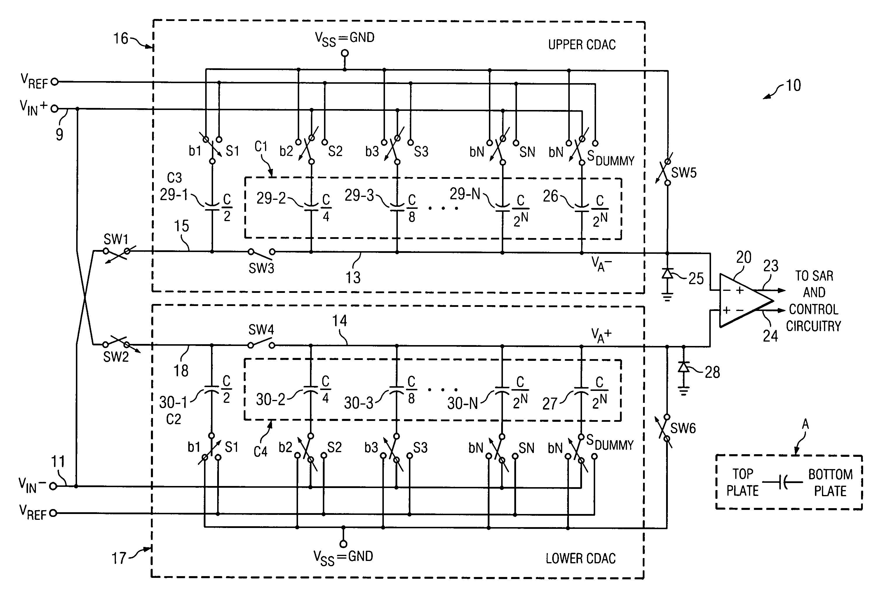
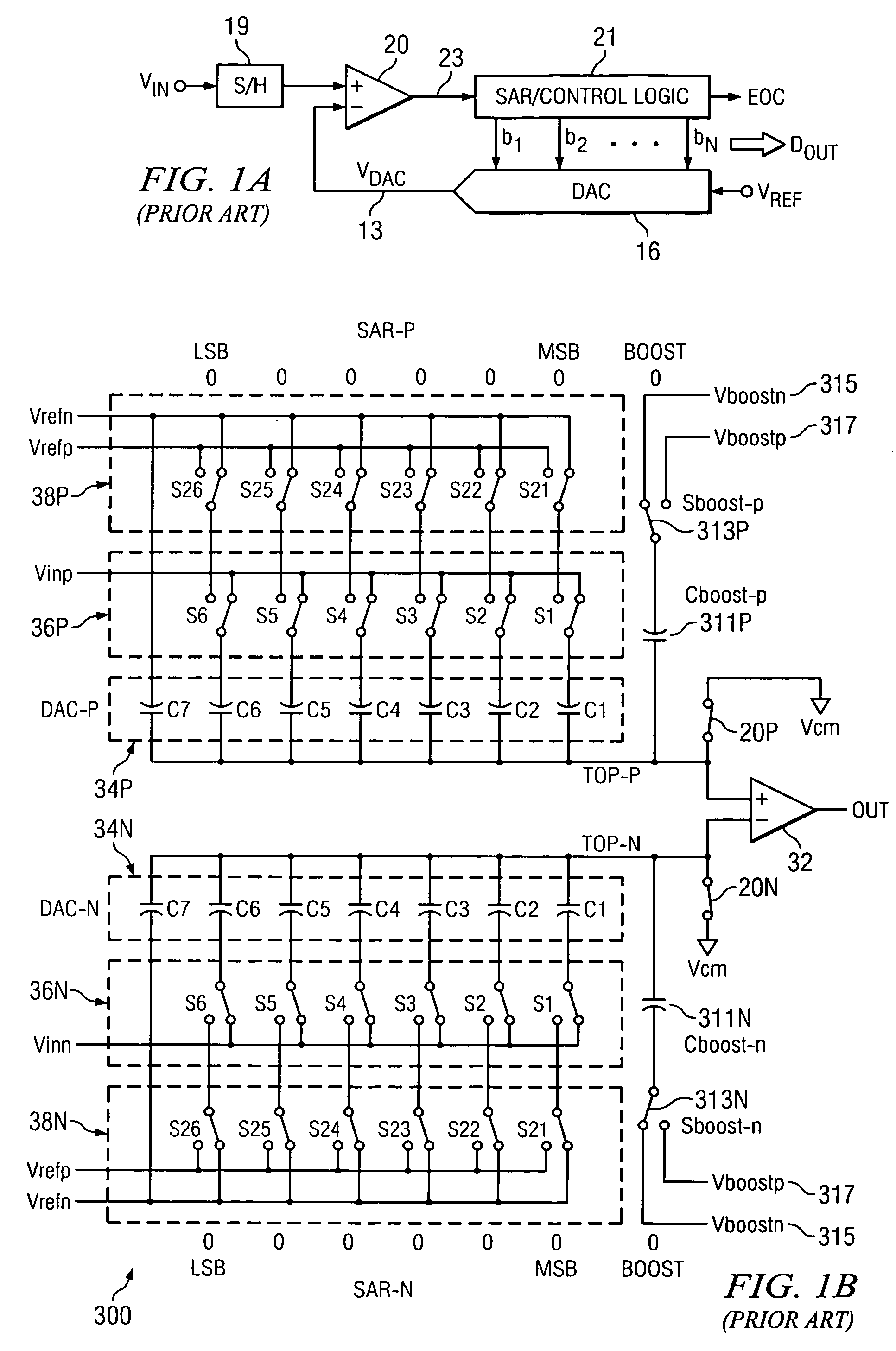
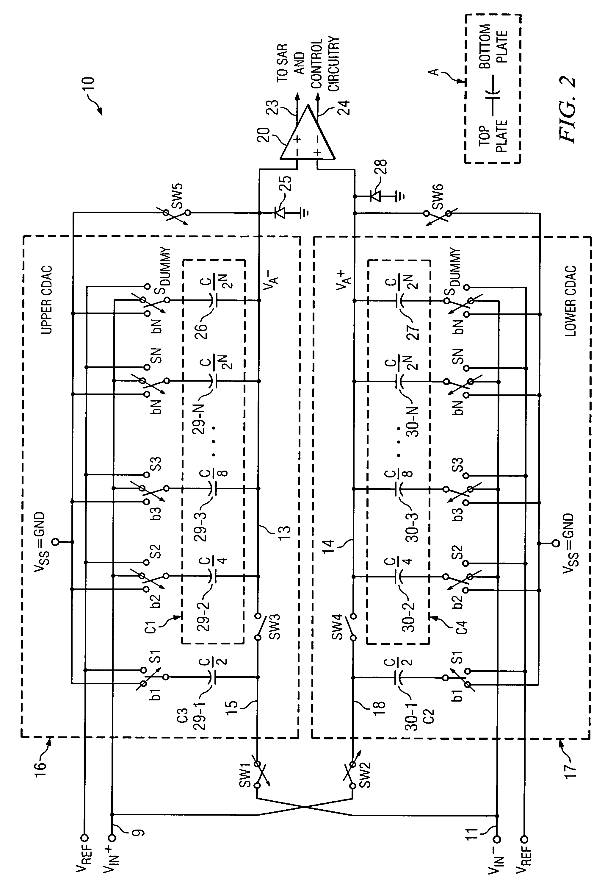
[0053]Referring to FIG. 2, SAR ADC 10 includes an upper CDAC (capacitor digital to analog converter) 16, a lower CDAC 17, and a conventional comparator 20. SAR ADC 10 also includes conventional SAR and control logic circuitry, such as SAR / control logic 21 shown in Prior Art FIG. 1. A differential analog input voltage VIN+−VIN− is applied between input conductors 9 and 11.

[0054]Upper CDAC 16 includes N binary weighted capacitors 29-1,2 . . . N, a dummy capacitor 26, N switches S1, S2 . . . SN, and a dummy switch SDUMMY. (In one implementation, N is equal to 16 (or equivalent to 16, for example, if conventional scaling capacitors are used). Capacitor 29-1 is the MSB capacitor of upper CDAC 16, and has its “top plate” connected to conductor 15 and its “bottom plate” connected to the pole terminal of switch S1. (Note the symbol “A” shown in FIG. 2 for a CDAC capacitor indicating which plate is the “top plate” and which plate is the “bottom plate”.) The remaining capacitors 29-2,3 . . . ...


PUM


Abstract

A switched-capacitor circuit (10, 32 or 32A) samples a first signal (VIN+) onto a first capacitor (C1 or CIN1) by switching a top plate thereof via a summing conductor (13) to a first reference voltage (VSS) and switching a bottom plate thereof to the first signal. A second signal (VIN) is sampled onto a second capacitor (C3 or CIN3) by switching a top plate thereof to the second signal and switching a bottom plate thereof to the first reference voltage. After the sampling, the top plate of the second capacitor is coupled to the top plate of the first capacitor. The bottom plate of the second capacitor is coupled to the first reference voltage. The bottom plate of the first capacitor is coupled to a second reference voltage (VDD or VREF), to thereby cancel at least a portion of a common mode input voltage component from the first conductor (13), hold the sampled differential charge on the summing conductor and establish a predetermined common mode voltage thereon, and prevent the summing conductor from having a voltage which allows the leakage of charge therefrom. The switched-capacitor circuit may be a SAR, an integrator, or an amplifier.

Description

BACKGROUND OF THE INVENTION[0001]The present invention relates generally to switched capacitor circuits, including SAR ADCs (successive approximation register analog to digital converters), and more particularly to an improved technique for avoiding charge leakage through integrated circuit substrate diodes caused by analog summing node voltages swinging outside of an acceptable range in a switched capacitor circuit, an SAR ADC, and still more particularly to SAR ADCs that are simpler and less expensive than those available in the prior art.[0002]Prior Art FIG. 1A is a simplified diagram of a basic well-known single-ended SAR ADC which executes a conventional SAR algorithm to convert an analog input voltage VIN to a digital output signal DOUT. For example, see FIGS. 13.5, 13.6, and 13.7 and associated text in “Analog Integrated Circuit Design” by David Johns and Ken Martin (1997 John Wiley & Sons, Inc.).[0003]The SAR ADC in Prior Art FIG. 1A includes a sample / hold circuit 19 that re...

Claims


Application Information

Patent Timeline
IPC IPC(8): H03M1/12H03M1/00
CPCH03M1/468H03M1/1295
Inventor WANG, YANKALTHOFF, TIMOTHY V.WU, MICHAEL A.
Owner TEXAS INSTR INC
Why Eureka
Try Eureka