Bi-section semiconductor laser device, method for manufacturing the same, and method for driving the same

a laser device and semiconductor technology, applied in the direction of lasers, semiconductor laser structure details, semiconductor lasers, etc., can solve the problems of easy misalignment between the second electrode increased operating voltage of laser devices, etc., to suppress the degradation of optical and electrical characteristics of the second compound semiconductor layer, high peak power, and high electrical resistance

Active Publication Date: 2012-11-08
SONY CORP +1
View PDF1 Cites 3 Cited by
  • Summary
  • Abstract
  • Description
  • Claims
  • Application Information

AI Technical Summary

Benefits of technology

[0012]In the method for manufacturing a bi-section semiconductor laser device disclosed in Patent Document 1, after a stacked structure is formed, a first metal film is formed on a second compound semiconductor layer. Subsequently, a second electrode is separated by a separating groove into a first portion and a second portion through dry etching of the first metal film. An etching mask is then formed, and a ridge structure is formed. In the method for manufacturing a bi-section semiconductor laser device disclosed in Patent Document 1, a ridge structure is not formed through self-alignment using the patterned second electrode as an etching mask. Therefore, misalignment is easily caused between the second electrode and the ridge structure. Furthermore, an oxidation film and impurities are easily left between the second compound semiconductor layer and the first metal film, which easily poses a problem in that the operating voltage of the laser device is increased as the contact resistance of the compound semiconductor layer and the metal film is increased.
[0013]In the method for manufacturing a bi-section semiconductor laser device disclosed in Patent Document 2, after a stacked structure is formed, an etching mask is formed and a ridge structure is formed. Subsequently, an insulating layer is formed on the side of the ridge structure, and a second electrode separated by a separating groove into a first portion and a second portion is formed by performing liftoff across the upper surface of the insulating layer and a second compound semiconductor layer. Therefore, in the method for manufacturing a bi-section semiconductor laser device disclosed in Patent Document 2, an oxidation film and impurities are also easily left between the second compound semiconductor layer and the first metal film, which easily poses a problem in that the operating voltage of the laser device is increased as the contact resistance of the compound semiconductor layer and the metal film is increased.
[0016]It is desirable to provide a method for manufacturing a bi-section semiconductor laser device that allows a ridge structure and a second electrode separated by a separating groove into a first portion and a second portion to be formed accurately, with certainty, and easily. It is also desirable to provide a bi-section semiconductor laser device that operates through self-pulsation with certainty when a light-emitting region is driven at a forward bias and a saturable absorption region is driven at a reverse bias independently and to provide a method for driving the bi-section semiconductor laser device.
[0036]In the method for manufacturing a bi-section semiconductor laser device according to an embodiment of the present invention, a ridge structure is formed by etching at least part of the second compound semiconductor layer using the belt-shaped second electrode as an etching mask. Since the ridge structure is formed through self-alignment using the patterned second electrode as an etching mask, misalignment is not caused between the second electrode and the ridge structure. In addition, a separating groove is formed in the second electrode by wet etching. By adopting wet etching but not dry etching, the degradation of the optical and electrical characteristics of the second compound semiconductor layer can be suppressed. Therefore, the light-emitting characteristics of the bi-section semiconductor laser device can be prevented from being degraded with certainty.
[0037]In the bi-section semiconductor laser device according to an embodiment of the present invention or in the bi-section semiconductor laser device used in the method for driving a bi-section semiconductor laser device according to an embodiment of the present invention, the electrical resistance between the first portion and the second portion of the second electrode is 10 times or more that between the second electrode and the first electrode or 1×10² Ω or more. Thus, a leakage current flowing from the first portion of the second electrode to the second portion can be suppressed with certainty. In other words, a reverse bias voltage applied to the saturable absorption region can be increased while at the same time a current injected into the light-emitting region (gain region) can be increased. This can achieve a self-pulsation operation in a single mode that has an optical pulse with high peak power. Furthermore, such a high electrical resistance between the first portion and the second portion of the second electrode can be achieved by only separating the second electrode into the first portion and the second portion by the separating groove. In other words, the optical pulse generation using mode locking can be easily achieved, which can provide a short pulse GaN semiconductor laser device, a light source of a volumetric optical disk system using the same, and a light source demanded in medical and bio-imaging fields.

Problems solved by technology

Therefore, misalignment is easily caused between the second electrode and the ridge structure.
Furthermore, an oxidation film and impurities are easily left between the second compound semiconductor layer and the first metal film, which easily poses a problem in that the operating voltage of the laser device is increased as the contact resistance of the compound semiconductor layer and the metal film is increased.
Therefore, in the method for manufacturing a bi-section semiconductor laser device disclosed in Patent Document 2, an oxidation film and impurities are also easily left between the second compound semiconductor layer and the first metal film, which easily poses a problem in that the operating voltage of the laser device is increased as the contact resistance of the compound semiconductor layer and the metal film is increased.
In the method for manufacturing a bi-section semiconductor laser device disclosed in Patent Document 3, the steps until the second electrode is formed are complicated and there are problems such as degradation in the electrical and optical characteristics of the surface of the p-side contact layer due to polishing, an increase in the operating voltage of the laser device caused by an increase in the contact resistance, and an increase in a threshold current and a decrease in a slope efficiency due to an increase in optical loss.

Method used


Image

  • Bi-section semiconductor laser device, method for manufacturing the same, and method for driving the same
  • Bi-section semiconductor laser device, method for manufacturing the same, and method for driving the same
  • Bi-section semiconductor laser device, method for manufacturing the same, and method for driving the same

Examples


example 2 (modification of example 1)

3. Example 2 (Modification of Example 1) and Others

[0057]Method for Manufacturing Bi-section Semiconductor Laser Device According to Embodiment of the Present Invention, Bi-section Semiconductor Laser Devices According to First and Second Embodiments of the Present Invention and Method for Driving the Devices, and General Description

[0058]In the method for manufacturing a bi-section semiconductor laser device according to an embodiment of the present invention, in the step (D), assuming that the etching rate of the second electrode is ER0 and the etching rate of the stacked structure is ER1 when the separating groove is formed in the second electrode, ER0 / ER124 1×10 is satisfied and ER0 / ER1≧1×10² is preferably satisfied. When ER0 and ER1 satisfy such a relationship, the second electrode can be etched with certainty while the stacked structure is not etched (or is slightly etched).

[0059]In this case, the second electrode is preferably composed of a palladium (Pd) single layer, a nick...

example 1

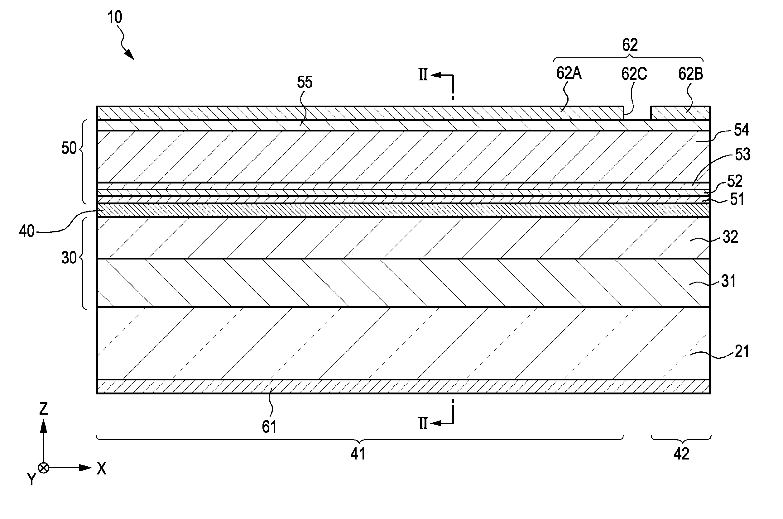
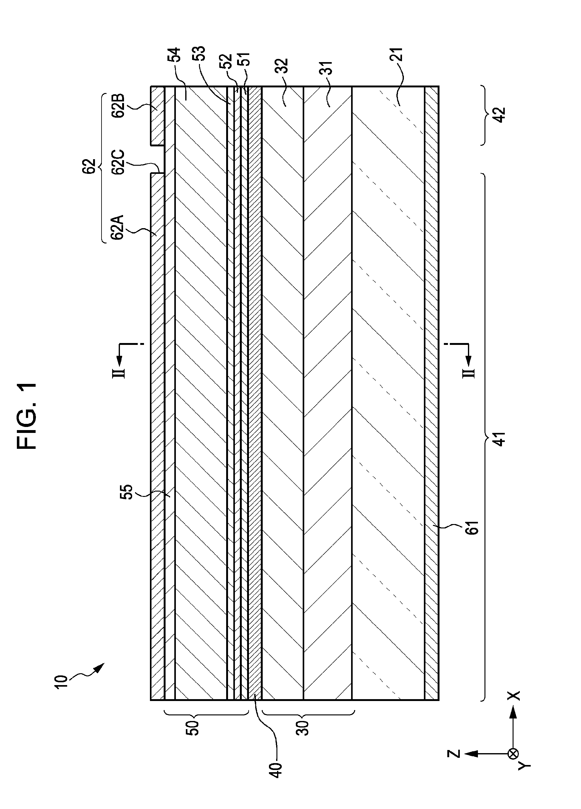
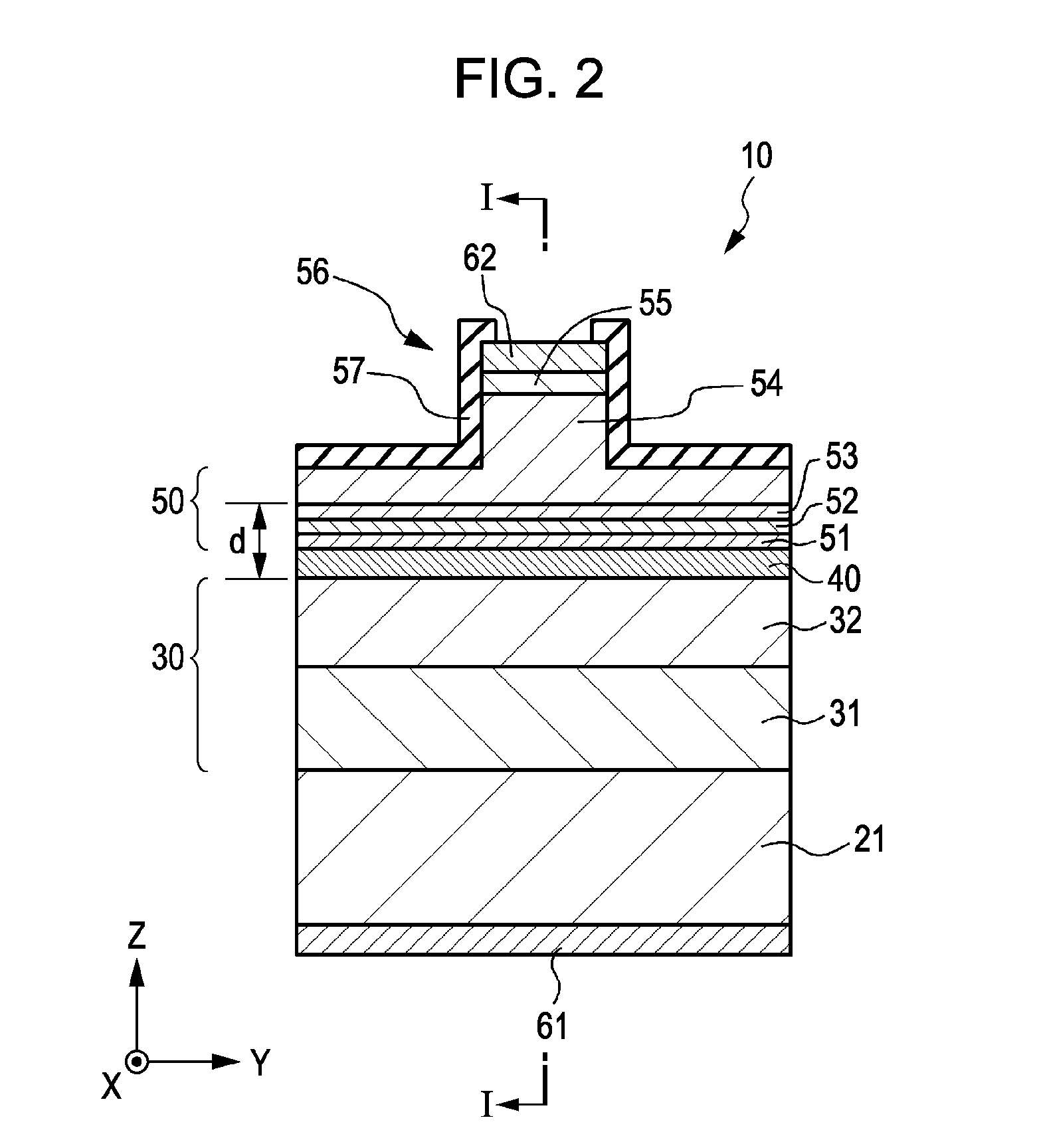
[0072]Example 1 relates to a method for manufacturing a bi-section semiconductor laser device according to an embodiment of the present invention, bi-section semiconductor laser devices according to first and second embodiments of the present invention, or a method for driving the same. FIG. 1 is a schematic end view (a schematic end view taken along an XZ plane) of a bi-section semiconductor laser device of Example 1 in a direction in which a cavity extends. FIG. 2 is a schematic sectional view (a schematic sectional view taken along a YZ plane) in a direction perpendicular to the direction in which the cavity extends. FIG. 1 is a schematic end view taken along line I-I of FIG. 2. FIG. 2 is a schematic sectional view taken along line II-II of FIG. 1.

[0073]A bi-section semiconductor laser device 10 of Example 1 having an emission wavelength of 405 nm includes:

[0074](a) a stacked structure obtained by stacking, in sequence, a first compound semiconductor layer 30 of a first conductiv...

example 2

[0102]Example 2 is a modification of Example 1. In Example 1, the bi-section semiconductor laser device 10 is disposed on the (0001) surface of an n-type GaN substrate 21, that is, on the C surface. The (0001) surface is a crystal face having a polarity. However, when such a substrate is used, the active layer 40 is subjected to a quantum confined Stark effect (QCSE) due to an internal electric field caused by piezoelectric polarization and spontaneous polarization, whereby it sometimes becomes difficult to electrically control saturable absorption. It was found that, in some cases, a direct current supplied to the first electrode and a reverse bias voltage applied to the saturable absorption region have to be increased in order to achieve self-pulsation and mode locking operations; a subpulse component accompanying a main pulse is generated; or it becomes difficult to achieve synchronization between external signals and optical pulses.

[0103]As a result, it was found that, to preven...


PUM


Abstract

A method for manufacturing a bi-section semiconductor laser device includes the steps of (A) forming a stacked structure obtained by stacking, on a substrate in sequence, a first compound semiconductor layer of a first conductivity type, a compound semiconductor layer that constitutes a light-emitting region and a saturable absorption region, and a second compound semiconductor layer of a second conductivity type; (B) forming a belt-shaped second electrode on the second compound semiconductor layer; (C) forming a ridge structure by etching at least part of the second compound semiconductor layer using the second electrode as an etching mask; and (D) forming a resist layer for forming a separating groove in the second electrode and then forming the separating groove in the second electrode by wet etching so that the separating groove separates the second electrode into a first portion and a second portion.

Description

RELATED APPLICATION DATA[0001]This application is a division of U.S. patent application Ser. No. 12 / 726,524, filed on Mar. 18, 2010, the entirety of which is incorporated herein by reference to the extent permitted by law. The present invention claims priority to and contains subject matter related to Japanese Patent Application Nos. JP 2009-077070 filed in the Japan Patent Office on Mar. 26, 2009 and JP 2010-031299 filed in the Japan Patent Office on Feb. 16, 2010, the entire contents both of which being incorporated herein by reference.BACKGROUND OF THE INVENTION[0002]1. Field of the Invention[0003]The present invention relates to a bi-section semiconductor laser device, a method for manufacturing the same, and a method for driving the same.[0004]2. Description of the Related Art[0005]It is expected that a high-power ultrashort-pulse semiconductor laser device that has an emission wavelength of 405 nm and is composed of a GaN compound semiconductor will realize a light source of a...

Claims


Application Information

Patent Timeline
Patent Type & Authority Applications(United States)
IPC IPC(8): H01S5/02
CPCB82Y20/00H01S5/0425H01S5/0602H01S5/0625H01S5/34333H01S5/14H01S5/22H01S5/3216H01S5/0658H01S5/04256
Inventor WATANABE, HIDEKIMIYAJIMA, TAKAOIKEDA, MASAOYOKOYAMA, HIROYUKIOKI, TOMOYUKIKURAMOTO, MASARU
Owner SONY CORP
Why Eureka
Try Eureka