

Light-emitting device and electronic device using the light-emitting device
- Summary
- Abstract
- Description
- Claims
- Application Information
AI Technical Summary
Benefits of technology
Problems solved by technology
Method used
Image

Examples
embodiment 1
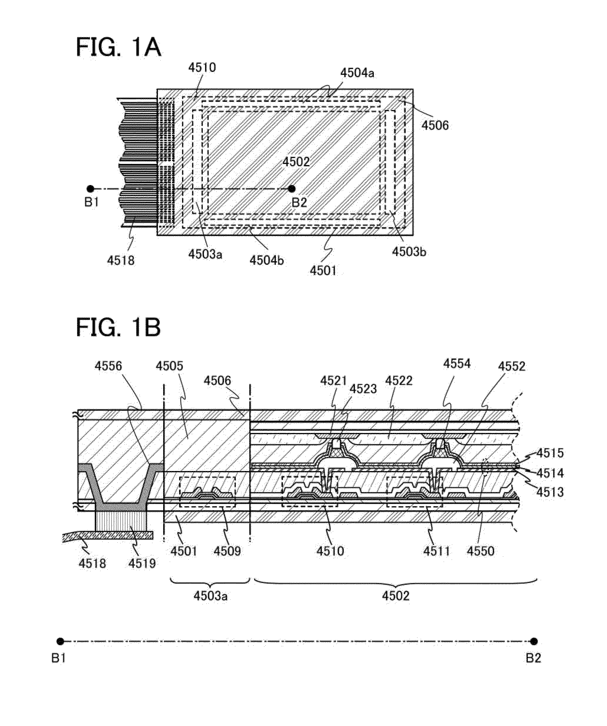
[0044]Next, an example of an active matrix Light-emitting device is described with reference to FIGS. 1A and 1B. Note that FIG. 1A is a top view of a light-emitting device and FIG. 1B is a cross-sectional view taken along dashed line B1-B2 in FIG. 1A.
[0045]The light-emitting device shown in FIG. 1A is provided with a pixel portion 4502, signal line driver circuits 4503a and 4503b, and scan line driver circuits 4504a and 4504b which are provided over a first substrate 4501. In addition, a second substrate 4506 is provided over the pixel portion 4502, the signal line driver circuits 4503a and 4503b, and the scan line driver circuits 4504a and 4504b.
[0046]Note that the first substrate 4501 and the second substrate 4506 are formed using flexible substrates.
[0047]Further, in the light-emitting device shown in FIG. 1B, transistors 4509, 4510, and 4511 arc formed over the first substrate 4501, and a light-emitting clement 4550 is formed over the transistors 4510 and 4511.
[0048]Light from ...
embodiment 2
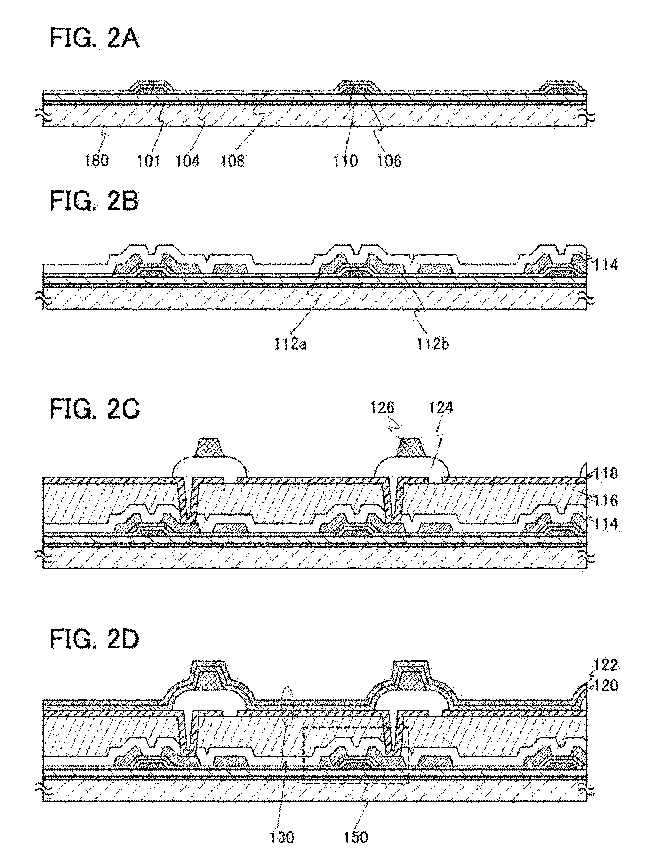
[0064]A method for manufacturing the light-emitting device illustrated in FIGS. 1A and 1B will be described with reference to FIGS. 2A to 2D, FIGS. 3A to 3C, FIGS. 4A and 4B, and FIGS. 5A and 5B.
[0065]First, a first separation layer 101 is formed over a third substrate 180, and a first buffer layer 104 is formed over the first separation layer 101. It is preferable that the first buffer layer 104 be formed successively so that the first separation layer 101 is not exposed to air. The successive formation prevents dust or impurities from entering a portion between the first separation layer 101 and the first buffer layer 104 (see FIG. 2A).
[0066]The third substrate 180 may be a glass substrate, a quartz substrate, a sapphire substrate, a ceramic substrate, a metal substrate, or the like. Alternatively, a plastic substrate which can withstand the processing temperature of this embodiment may be used. In the case where a plastic substrate is used, the separation layer 101 is not necessa...
embodiment 3
[0140]Structures of a spacer, a coloring layer, and a fixed portion which are used in the light-emitting device of this invention, which are different from those of the spacer 126, the coloring layer 166, and the fixed portion 168 which are described in Embodiment 2, are described with reference to FIGS. 6A to 6C.
[0141]Note that the same reference numerals are used for the same parts as those of the light-emitting device in Embodiment 1, and description of the parts with the same reference numerals will be omitted here.
[0142]A light-emitting device in FIG. 6A is an example in which a spacer 208 is bonded to the first bonding layer 170 by welding and also bonded to the partition 124 by welding by laser light irradiation. A material which absorbs visible light is added to the spacer 208, and the spacer 208 is firmly fixed to the first bonding layer 170 and the partition 124. Further, the light-emitting layer 120 formed on the top surface and part of the side surface is separated by th...
PUM
 Abstract
Description
Claims
Application Information