Non-volatile memory device and sensing method thereof

a non-volatile memory and sensing technology, applied in the field of non-volatile memory devices and sensing methods thereof, can solve the problems of increased noise, difficulty in application or implementation, and difficulty in current flow between the top electrode b>1/b> and the bottom electrode b>3/b>, so as to reduce the number of times that a read operation is performed, reduce the number of circuit areas, and reduce the effect of nois

Active Publication Date: 2012-11-15
SK HYNIX INC
View PDF2 Cites 70 Cited by
  • Summary
  • Abstract
  • Description
  • Claims
  • Application Information

AI Technical Summary

Benefits of technology

[0043]First, since an embodiment of the present invention detects a difference in time at which a precharged bit line is discharged in response to a cell resistance value to sense multi-level data, it is possible to reduce the number of times that a read operation is performed and to implement a simple control mechanism for a verification operation, thereby reducing a circuit area related to the control of the read operation.
[0044]Seco...

Problems solved by technology

As a result, it is difficult for the current to flow between the top electrode 1 and the bottom electrode 3.
However, if the number of bits of read data increases, the number of times the read operation is performed for one cell should be increased, or several reference voltage levels should be applied according to a sensing scheme, resulting...

Method used


Image

  • Non-volatile memory device and sensing method thereof
  • Non-volatile memory device and sensing method thereof
  • Non-volatile memory device and sensing method thereof

Examples


Embodiment Construction

[0059]Reference will now be made in detail to the embodiments of the present invention, examples of which are illustrated in the accompanying drawings. Wherever possible, the same reference numbers will be used throughout the drawings to refer to the same or like parts.

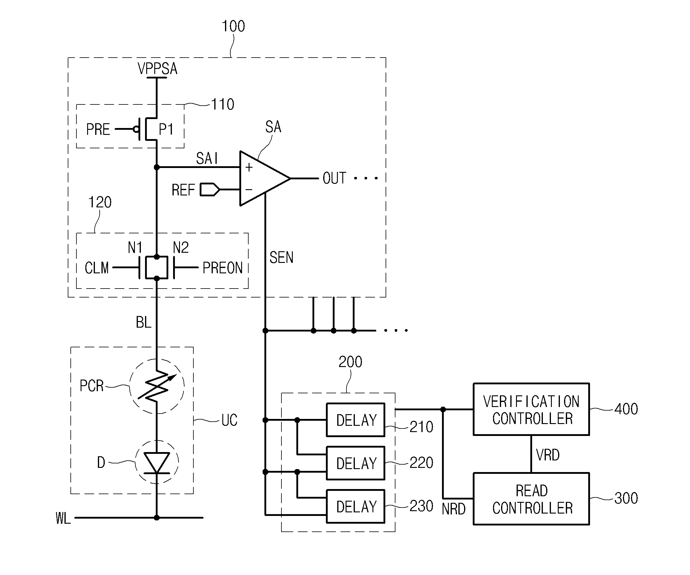
[0060]FIG. 7 is a circuit diagram illustrating a non-volatile memory device according to an embodiment of the present invention.

[0061]Referring to FIG. 7, the non-volatile memory device includes a sensing unit 100, a unit cell UC, a sensing controller 200, a read controller 300, and a verification controller 400.

[0062]In this embodiment, the sensing unit 100 includes a precharge unit 110, a clamping unit 120, and a sense amplifier SA. The sensing controller 200 includes a plurality of delay units 210 to 230. The non-volatile memory device includes a plurality of unit cells UCs to make a cell array. Each unit cell UC may include a phase change resistor (PCR) element and a diode D. The PCR element is coupled to and disp...


PUM


Abstract

A non-volatile memory device and a sensing method thereof are disclosed, which can sense multi-level data using resistance variation. The non-volatile memory device includes a cell array and a sensing unit. The cell array includes a plurality of unit cells where data is read out or written. The sensing unit compares a sensing voltage corresponding to data stored in the unit cell with a reference voltage, amplifies/outputs the compared result, measures a difference in discharge time where the sensing voltage is discharged in response to a resistance value of the unit cell during an activation period of a sensing enable signal after a bit line is precharged, and senses the data in response to the measured result.

Description

CROSS-REFERENCE TO RELATED APPLICATION[0001]The priority of Korean patent application No. 10-2011-0044206 filed on May 11, 2011, the disclosure of which is hereby incorporated in its entirety by reference, is claimed.BACKGROUND OF THE INVENTION[0002]Embodiments of the present invention relate to a non-volatile memory device and a sensing method thereof, and more specifically, to a non-volatile memory device configured to sense multi-level data using resistance variation.[0003]Memory devices may be classified into volatile memory devices and non-volatile memory devices. Non-volatile memory devices include a non-volatile memory cell capable of preserving stored data even when not powered. For example, a non-volatile memory device may be implemented as a flash random access memory (flash RAM), a phase change random access memory (PCRAM), or the like.[0004]A PCRAM includes a memory cell that is implemented using a phase change material such as germanium antimony tellurium (GST), wherein...

Claims


Application Information

Patent Timeline
IPC IPC(8): G11C7/12G11C7/00
CPCG11C11/5607G11C11/5642G11C11/5657G11C11/5678G11C11/5685G11C2013/0054G11C13/0004G11C13/004G11C13/0061G11C13/0064G11C13/0002G11C16/04G11C16/06G11C16/26G11C16/32
Inventor KIM, DONG KEUN
Owner SK HYNIX INC
Why Eureka
Try Eureka