High-Gain Complementary Inverter with Ambipolar Thin Film Transistors and Fabrication Thereof

a technology of ambipolar thin film transistor and complementary inverter, which is applied in the field of high-gain complementary inverter with ambipolar thin film transistor and fabrication thereof, can solve the problems of amorphous thin, large operation voltage, and lower carrier mobility, and achieves large operation voltage, unsteady electric characteristics, and low carrier mobility

Active Publication Date: 2012-11-29
NAT CHIAO TUNG UNIV
View PDF1 Cites 8 Cited by
  • Summary
  • Abstract
  • Description
  • Claims
  • Application Information

AI Technical Summary

Benefits of technology

[0004]In the known technology, the material of the active layer used in the thin film semiconductor element used for manufacturing the glass substrate or the display panel is almost the inorganic amorphous or polysilicon material. However, the amorphous thin film has disadvantages as follows: the lower carrier mobility, the larger operation voltage and the unsteady electric characteristics. The polysilicon thin film has disadvantages as follows: the higher cost, the complicated manufacture and the device uniformity is not good. In order to resolve the problems mentioned above, in one embodiment, the present invention provides an ambipolar thin film transistor, comprising: a gate layer, wherein material of the gate layer is low-resistivity Si or metal conductor, and wherein the metal conductor is aluminum (Al), molybdenum (Mo), titanium (Ti), wolfram(W) or the related alloys; a silica layer, forming on the gate layer; an active layer, forming on the silica layer, wherein the active layer is formed by stacking up a n-type semiconductor thin film and a p-type semiconductor thin film; a source, forming on the gate layer and connecting to one side of the active layer; and a drain, forming on the gate layer, connecting to another side of the active layer and corresponding to the source.
[0005]In another embodiment, the present invention provides a high gain complementary inverter with ambipolar thin film transistors, comprising: a gate layer, wherein material of the gate layer is low-resistivity Si or metal conductor, and wherein the metal conductor is aluminum (Al), molybdenum (Mo), titanium (Ti), wolfram (W) or the related alloys; a silica layer, forming on the gate layer; a first active layer, forming on the silica layer, wherein the active layer is formed by stacking up a first n-type semiconductor thin film and a first p-type semiconductor thin film; a first source, forming on the gate layer and connecting to one side of the first active layer; a first drain, forming on the gate layer, connecting to another side of the first active layer and corresponding to the first source; a second active layer, forming on the silica layer, wherein the second active layer is formed by stacking up a second n-type semiconductor thin film and a second p-type semiconductor thin film; a second source, forming on the gate layer and connecting to one side of the second active layer; and a second drain, forming on the gate layer, connecting to another side of the second active layer and corresponding to the second source.
[0006]Further scope of applicability of the present application will become more apparent from the detailed description given hereinafter. However, it should be understood that the detailed description and specific examples, while indicating exemplary embodiments of the disclosure, are given by way of illustration only, since various changes and modifications within the spirit and scope of the disclosure will become apparent to those skilled in the art from this detailed description.

Problems solved by technology

However, the amorphous thin film has disadvantages as follows: the lower carrier mobility, the larger operation voltage and the unsteady electric characteristics.
The polysilicon thin film has disadvantages as follows: the higher cost, the complicated manufacture and the device uniformity is not good.

Method used


Image

  • High-Gain Complementary Inverter with Ambipolar Thin Film Transistors and Fabrication Thereof
  • High-Gain Complementary Inverter with Ambipolar Thin Film Transistors and Fabrication Thereof
  • High-Gain Complementary Inverter with Ambipolar Thin Film Transistors and Fabrication Thereof

Examples


Embodiment Construction

[0018]For your esteemed members of reviewing committee to further understand and recognize the fulfilled functions and structural characteristics of the disclosure, several exemplary embodiments cooperating with detailed description are presented as the follows.

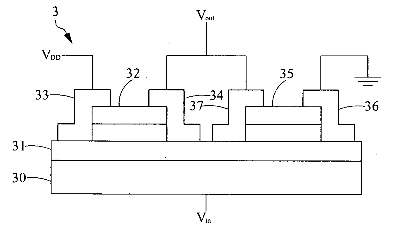
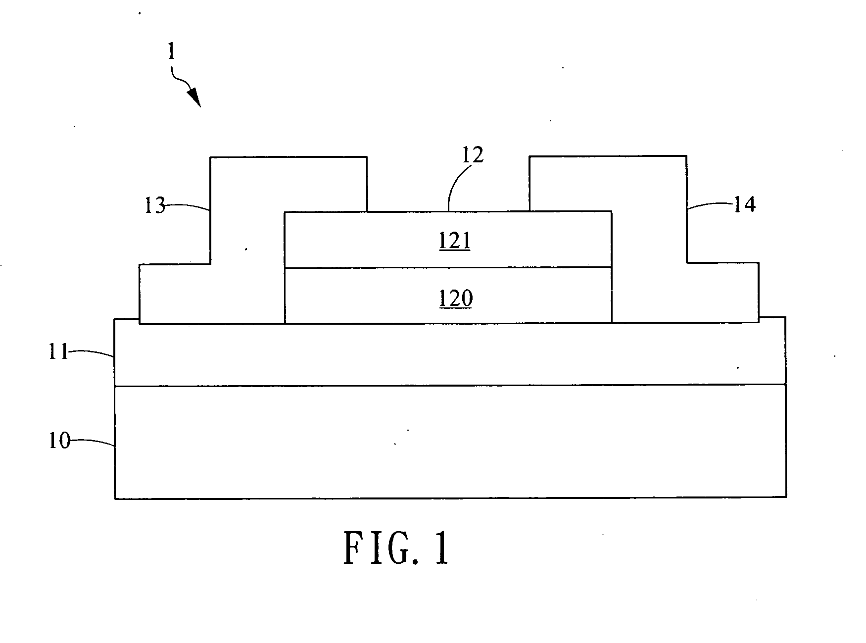
[0019]FIG. 1 is a schematic diagram showing an ambipolar thin film transistor 1 according to one embodiment of the present invention. The ambipolar thin film transistor 1 comprises: a gate layer 10, wherein material of the gate layer 10 is low-resistivity Si or metal conductor, and wherein the metal conductor is aluminum (Al), molybdenum (Mo), titanium (Ti), wolfram (W) or the related alloys; a silica layer 11, forming on the gate layer 10; an active layer 12, forming on the silica layer 11, wherein the active layer 12 is formed by stacking up a n-type semiconductor thin film 120 and a p-type semiconductor thin film 121. The active layer 12 simultaneously has the n-type and p-type thin films, so electrons or holes may be tran...


PUM

PropertyMeasurementUnit
temperatureaaaaaaaaaa
resistivityaaaaaaaaaa

Abstract

The present invention relates to a high gain complementary inverter with ambipolar thin film transistors and fabrication thereof, comprising: a gate layer, a silica layer, a first active layer, a first source, a first drain, a second active layer, a second source and a second drain for fabrication cost and complexity reduction.

Description

TECHNICAL FIELD[0001]The present invention relates to a complementary inverter with ambipolar thin film transistors, and more particularly, to a high gain complementary inverter with ambipolar thin film transistors that can be used in semiconductor and photoelectronic industry, for example, a flat panel display.TECHNICAL BACKGROUND[0002]With rapid development of the flat panel display, the application of the thin film transistor (TFT) has achieved great recognition. The thin-film element is configured to replace with the external integrated circuit (IC) module so as to completely manufacture circuits with various functions on the system on panel (SOP) in flat panel display. This technology is widely developed for achieving some goals, for example, the product with thin, light and low cost and the high manufacturing yield.[0003]In SOP technology, most function circuits composes of the unit circuit comprising TFT elements, for example, the phase inverter (or simply called inverter), t...

Claims


Application Information

Patent Timeline
Patent Type & Authority Applications(United States)
IPC IPC(8): H01L33/08
CPCH01L27/1225H01L29/7869H01L27/286H01L51/0036H01L29/78696H10K19/20H10K85/113
Inventor LIU, PO-TSUNCHOU, YI-TEHTENG, LI-FENGFU, CHUR-SHYANGSHIEH, HAN-PING
Owner NAT CHIAO TUNG UNIV
Why Eureka
Try Eureka