Mould for lithography by nano-imprinting and manufacturing methods

a technology of nano-imprinting and moulds, applied in nanotechnology, dough shaping, baking, etc., can solve the problems of difficult or impossible to obtain uniform contact, difficult to manufacture moulds by lithography and etching, and difficult to achieve uniform conta

Inactive Publication Date: 2012-11-29
COMMISSARIAT A LENERGIE ATOMIQUE ET AUX ENERGIES ALTERNATIVES
View PDF7 Cites 5 Cited by
  • Summary
  • Abstract
  • Description
  • Claims
  • Application Information

AI Technical Summary

Problems solved by technology

However, it is sometimes necessary to use material which is difficult to structure, such as silica or quartz, for example when it is desired to obtain a mould which is transparent to UV radiation.
In this case manufacture of the mould by lithography and etching becomes increasingly problematic the greater the resolution (resolutions of less than or equal to a few tens of nanometres).
In addition, use of a rigid mould makes the imprinting of patterns with satisfactory uniformity very difficult or impossible: the more rigid the mould the more it becomes difficult to obtain uniform contact (or conformal contact) at all points between a rigid mould and the substrate to be etched.
The disadvantage of this solution is that it requires that a uniform residual thickness is obtained in order to achieve a transfer of the patterns whilst retaining the lateral dimensions of the patterns.
However, we have just demonstrated that the maximum area of a mould was limited by its rigidity.
However, the resolution of such a mould is limited to 0.5 micrometre due to the problems of mechanical stability of the mould during pressing: small-sized patterns (typically less than 500 nm) do not have sufficient mechanical stability to resist during the pressing, which causes several types of mechanical deformation of the mould, limiting thereby the mould's potential resolution.
A mould made of PDMS cannot therefore be used to produce structures having resolutions of several nanometres, or even several tens of nanometres.
However, too great a rigidity or elastic modulus can make the material brittle and limit its capacity to generate conformal contact with the substrate to be imprinted.
In addition, the use of PDMS by thermal crosslinking remains an intrinsic limit for the manufacture of moulds having very high resolution.
Indeed, the cooling cycle of PDMS can cause mechanical stresses in the material, and consequently limit its resolution.

Method used


Image

  • Mould for lithography by nano-imprinting and manufacturing methods
  • Mould for lithography by nano-imprinting and manufacturing methods
  • Mould for lithography by nano-imprinting and manufacturing methods

Examples


Embodiment Construction

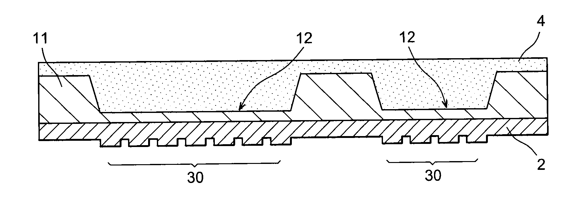
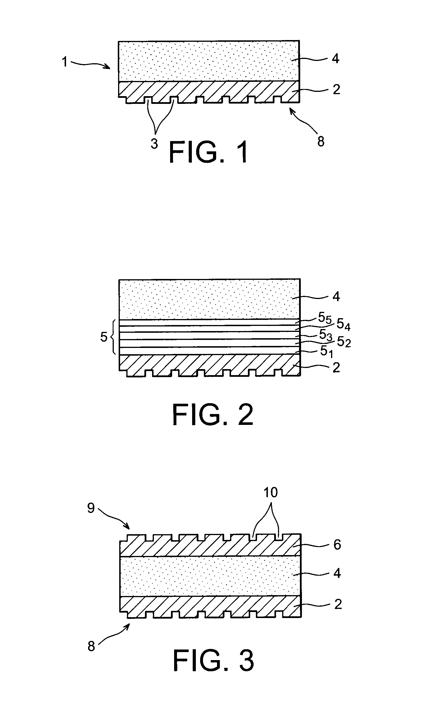
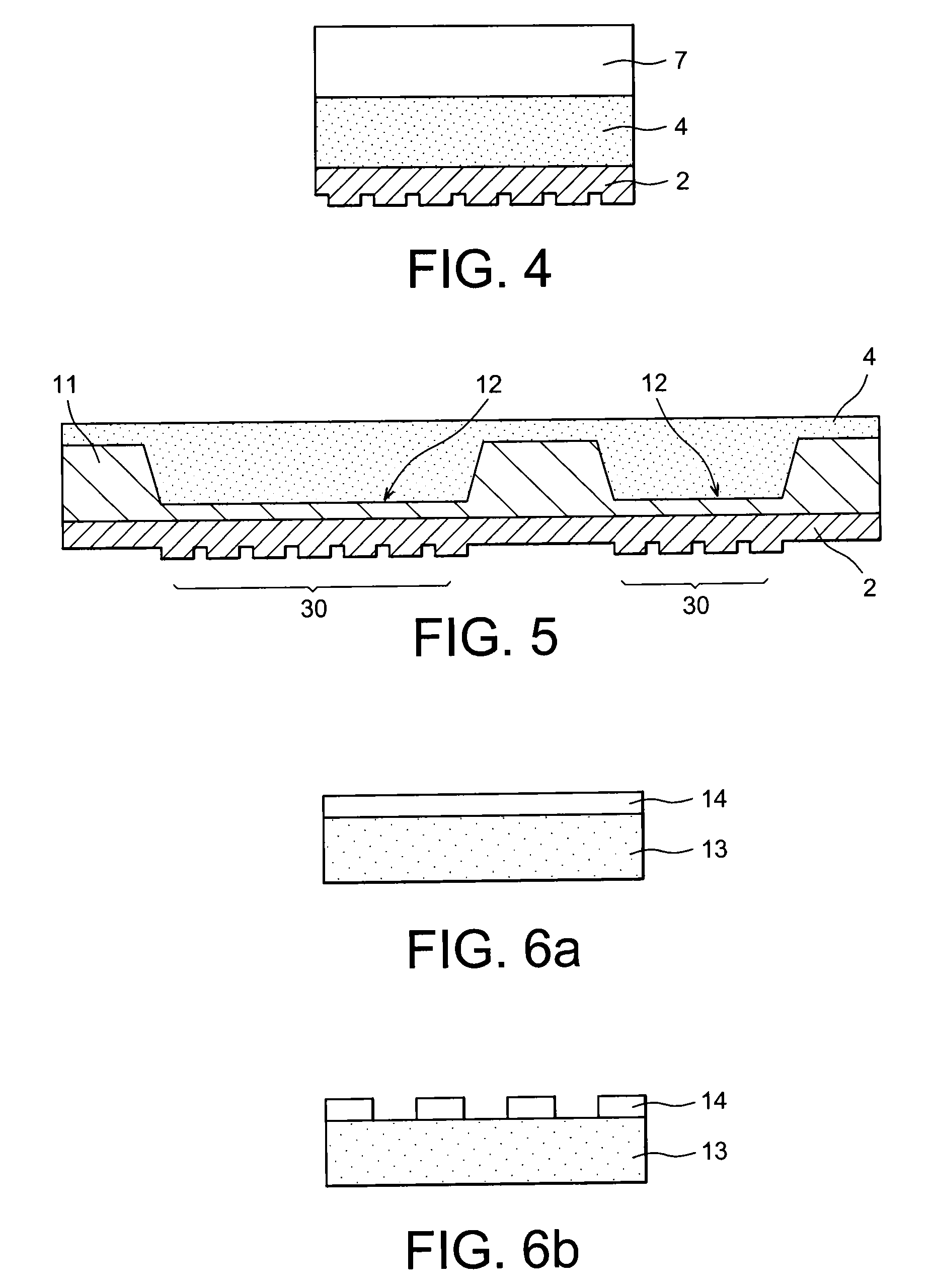
[0016]This aim is achieved by means of a mould for lithography by nano-imprinting having a first structured face including n structured zone(s) with patterns of micrometric or nanometric size, where n is an integer greater than or equal to 1, characterised in that the said first structured face belongs to a first layer which is supported by a second layer, and where the first layer is made of a rigid material and the second layer is made of a flexible material.

[0017]In the foregoing and in what follows the expression “structured with patterns of micrometric on nanometric size”, applied to a face or a layer, means that the face or the layer in question includes patterns, at least one dimension of which, of its length, its width and its diameter, is less than 1 mm and greater than 1 μm, in the case of patterns of micrometric size, and is greater than or equal to 1 nanometre and less than 1000 nanometres in the case of patterns of nanometric size.

[0018]In the context of the invention t...


PUM

PropertyMeasurementUnit
diameteraaaaaaaaaa
areasaaaaaaaaaa
sizeaaaaaaaaaa

Abstract

The invention concerns a mould for lithography by nano-imprinting, together with its manufacturing methods. This mould has a face which includes n structured zone(s) with patterns of micrometric or nanometric size, where n is an integer greater than or equal to 1. This structured face belongs to a first layer which is supported by a second layer, where the first layer is made of a rigid material and the second layer is made of a flexible material.
This mould may also include n intervening layers positioned between the first layer and the second layer, where n is an integer greater than or equal to 1, and in which the Young's modulus of the second layer is lower than the Young's modulus of the nth intervening layer adjacent to the second layer, and if n is greater than 1, the Young's modulus of the (i)th intervening layer is greater than the Young's modulus of the (i+1)th intervening layer, with i=1 to (n−1).

Description

TECHNICAL FIELD[0001]The invention concerns a mould for lithography by nano-imprinting, together with the methods for manufacturing such a mould.STATE OF THE PRIOR ART[0002]There are two types of lithography by nano-imprinting:[0003]nano-imprinting assisted by wavelength;[0004]thermal nano-imprinting.[0005]Lithography by nano-imprinting consists, in the case of thermal nano-imprinting, in duplicating patterns by hot pressing a mould in a polymer film positioned on a substrate for imprinting or, in the case of nano-imprinting assisted by wavelength, in duplicating patterns by pressing a mould, which is transparent to the mould's operating wavelength, in a photosensitive polymer film positioned on a substrate, and application of radiation of an operating wavelength (for example, a UV radiation) through the mould. The patterns reproduced in the polymer film are then etched in the substrate for imprinting underlying the polymer film.[0006]It is stipulated that nano-imprinting designates...

Claims


Application Information

Patent Timeline
Patent Type & Authority Applications(United States)
IPC IPC(8): B29C59/02B82Y40/00
CPCB82Y10/00G03F7/0002B82Y40/00
Inventor LANDIS, STEFAN
Owner COMMISSARIAT A LENERGIE ATOMIQUE ET AUX ENERGIES ALTERNATIVES
Why Eureka
Try Eureka