

Process for Enhanced 3D Integration and Structures Generated Using the Same
a technology structures, applied in the direction of electrical apparatus construction details, electromagnetic transmission, transmission, etc., can solve the problems of low input/output density, signal delay, and difficulty in powering the system through edge connections, and achieve the effect of enhanced 3d integration
- Summary
- Abstract
- Description
- Claims
- Application Information
AI Technical Summary
Benefits of technology
Problems solved by technology
Method used
Image

Examples
Embodiment Construction
[0002]1. Field of the Invention
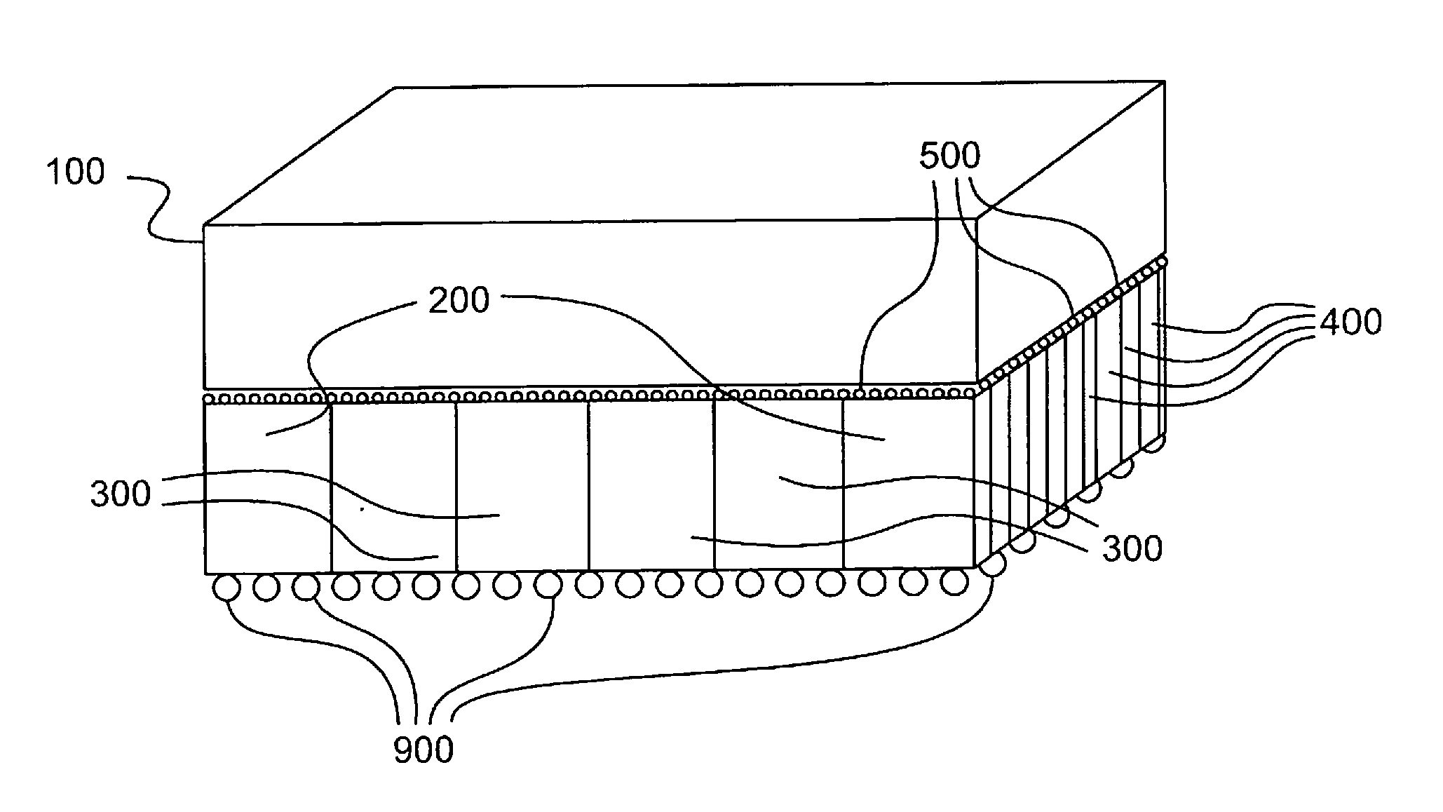
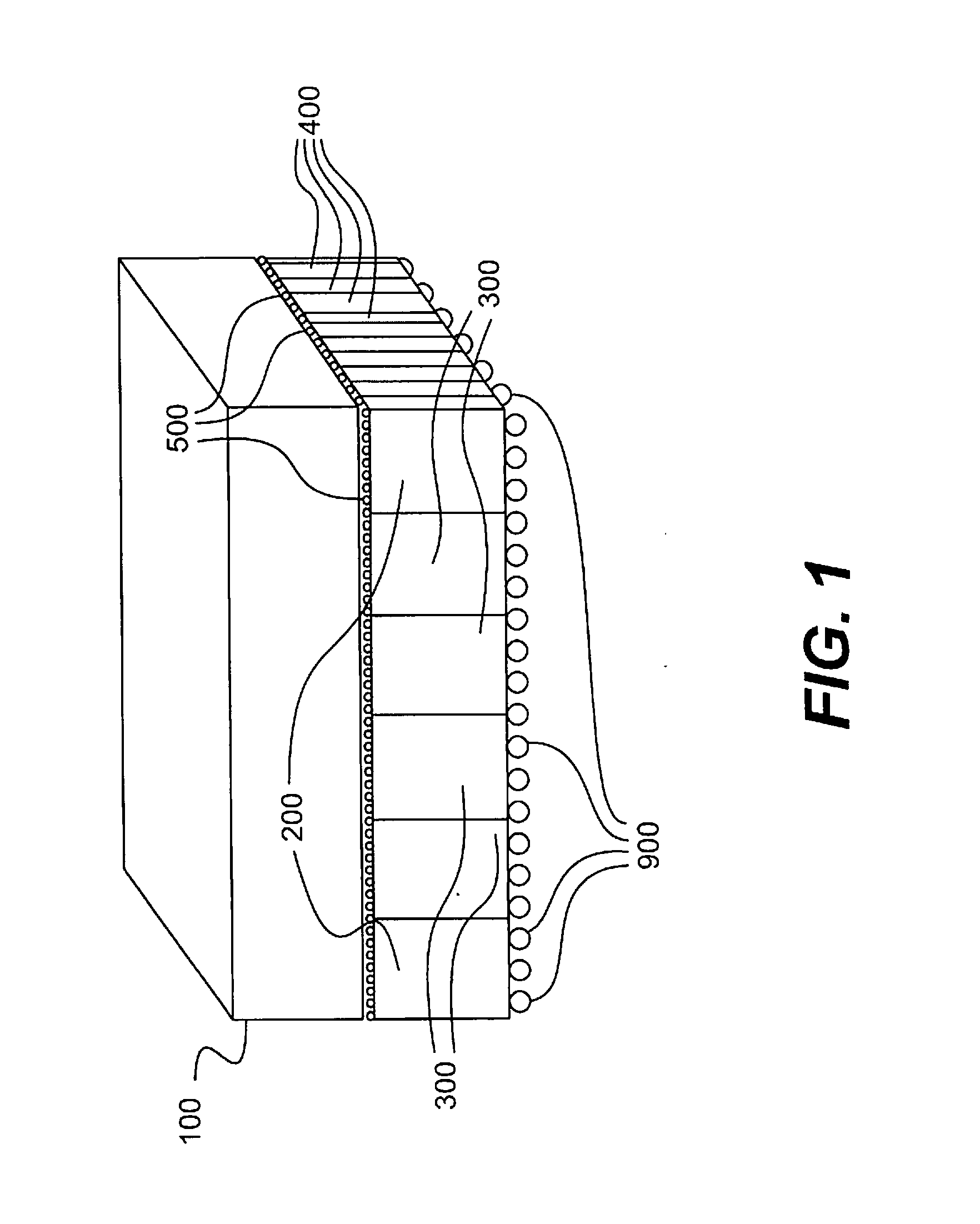
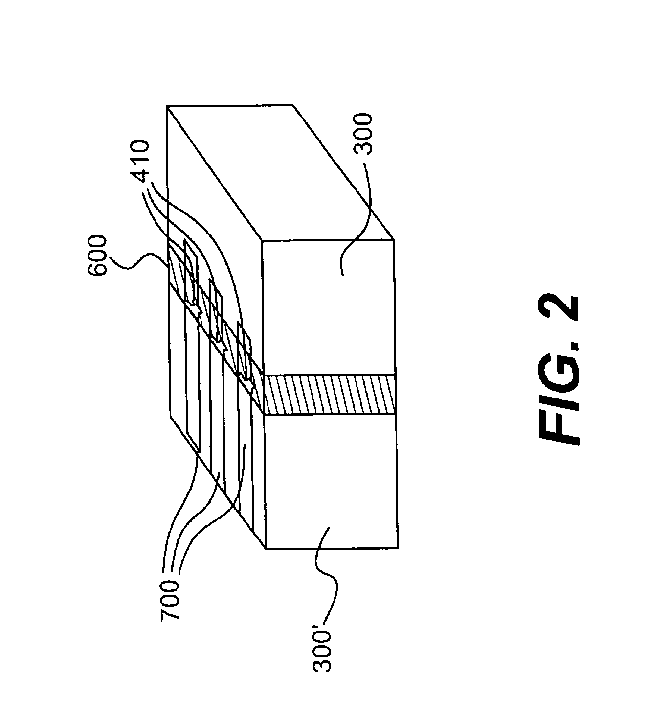
[0003]The field of the invention comprises integrated electronic 3D system devices and a process for building integrated 3D system devices that enables a higher level of system integration than possible with current 3D integration processes and structures, but does not employ through silicon vias.
[0004]2. Background of the Invention and Related Art
[0005]Various processes and structures described in the related art address high level system integration such as Hoffman, et al., U.S. Pat. No. 6,033,931, one of a class of so-called “cube patents.” Hoffman, et al. discloses a three-dimensional microchip circuit assembly process that employs a three-layer dry film sandwich to prepare a stacked circuit cube. Bertin, et al. U.S. Pat. No. 5,563,086 discloses an integrated memory cube structure and method of fabrication in which stacked semiconductor memory chips are integrated by a controlling logic chip such that a more powerful memory architecture is defined ...
PUM
| Property | Measurement | Unit |
|---|---|---|
| size | aaaaa | aaaaa |
| size | aaaaa | aaaaa |
| thickness | aaaaa | aaaaa |
Abstract
Description
Claims
Application Information