Method of manufacturing multilayer wiring substrate, and multilayer wiring substrate

a manufacturing method and wiring technology, applied in the direction of printed circuit aspects, circuit inspection/indentification, conductive pattern formation, etc., can solve the problems of increasing the number of terminals, narrowing of the inter-terminal pitch in the ic chip, and difficulty in connecting directly the ic chip to the mother board, so as to suppress the increase in manufacturing cost and suppress the manufacturing cost

Inactive Publication Date: 2012-12-13
NGK SPARK PLUG CO LTD
View PDF0 Cites 36 Cited by
  • Summary
  • Abstract
  • Description
  • Claims
  • Application Information

AI Technical Summary

Benefits of technology

[0022]According to the present invention as described in means 2, the recognition mark is formed on the principal plane of the substrate which provides the plane on which the chip components are mounted according to the difference in shades of color of the resin surface. In this case, since the recognition mark can be recognized without formation of the conductor layer and the opening section as in the case of the conventional art, the manufacturing cost of the multilayer wiring substrate can be suppressed.
[0023]The multilayer wiring substrate may, furthermore, include a conductor section which is exposed onto an outer edge section of the principal plane of the substrate and a positioning mark which is recognized according to a difference in an optical reflectance between the resin surface of one of the resin insulating layers which is the outermost layer and the surface of the conductor section. In this case, the recognition mark according to the difference in the shades of the color and the positioning mark according to the difference in the optical reflectance can be formed according to purposes. It should be noted that if, with the number of forming positioning marks according to the difference in the optical reflectance as a minimum limit, the other recognition marks are formed according to the difference in the shades of the color, the increase in the manufacturing cost can be suppressed to be low. In addition, the recognition marks formed according to the difference in the shades of color can be utilized as positioning marks for chip components and so forth.

Problems solved by technology

In this addition, there is a tendency of becoming increased number of terminals and of narrowing inter-terminal pitches in the IC chip.
However, since a large difference in the inter-terminal pitch is present between the terminal group of the IC chip and the terminal group of the mother board side, it is difficult to connect directly the IC chip onto the mother board.

Method used


Image

  • Method of manufacturing multilayer wiring substrate, and multilayer wiring substrate
  • Method of manufacturing multilayer wiring substrate, and multilayer wiring substrate
  • Method of manufacturing multilayer wiring substrate, and multilayer wiring substrate

Examples


third embodiment

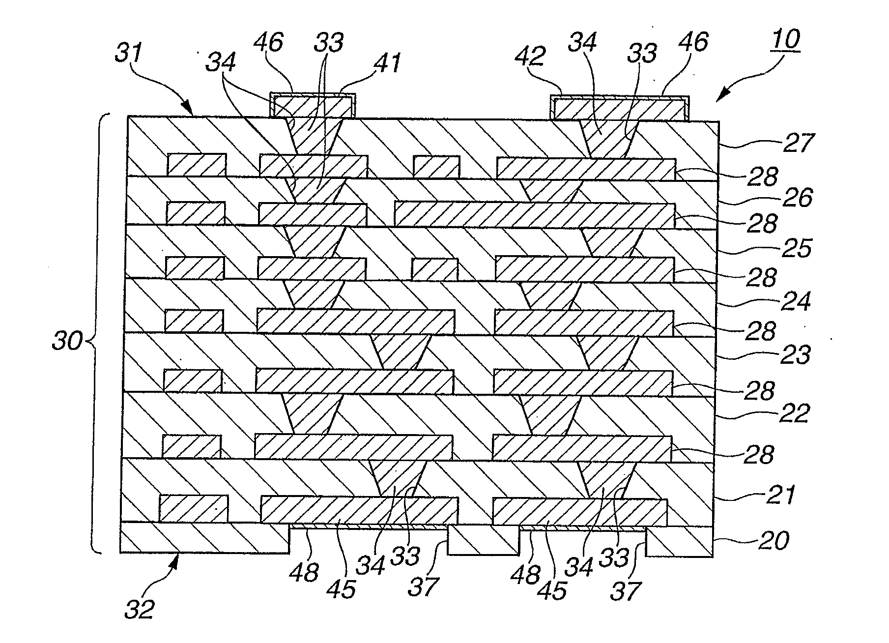
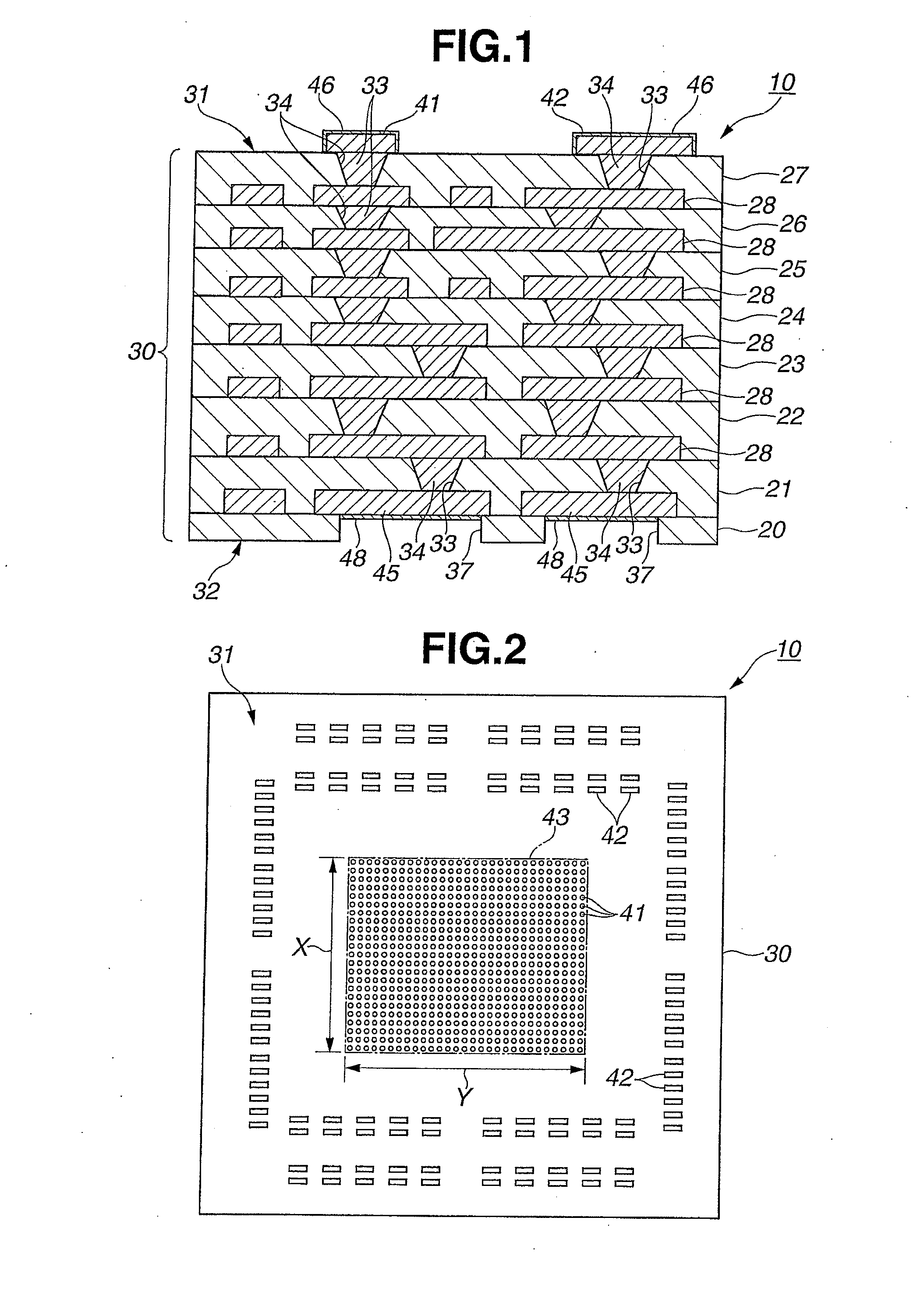
[0133]A third preferred embodiment which embodies the second feature according to the present invention will be described in details on a basis of the attached drawings. FIG. 20 is an expanded cross sectional view representing a rough configuration of the multilayer wiring substrate in the third preferred embodiment. FIG. 21 is a plan view of the multilayer wiring substrate viewed from the upper surface side

[0134]As shown in FIGS. 20 and 21, multilayer wiring substrate 10 in the third preferred embodiment is the coreless wiring substrate formed so as not to include the core substrate.

[0135]The basic structure and the preparation procedure on this multilayer wiring substrate are the same as those of the first preferred embodiment. Hence, the structure and the preparation procedure which are different only from the first embodiment will, hereinafter, be described.

[0136]As shown in FIG. 21, in multilayer wiring substrate 10, outermost resin insulating layer 27 exposed onto upper surfac...

fourth embodiment

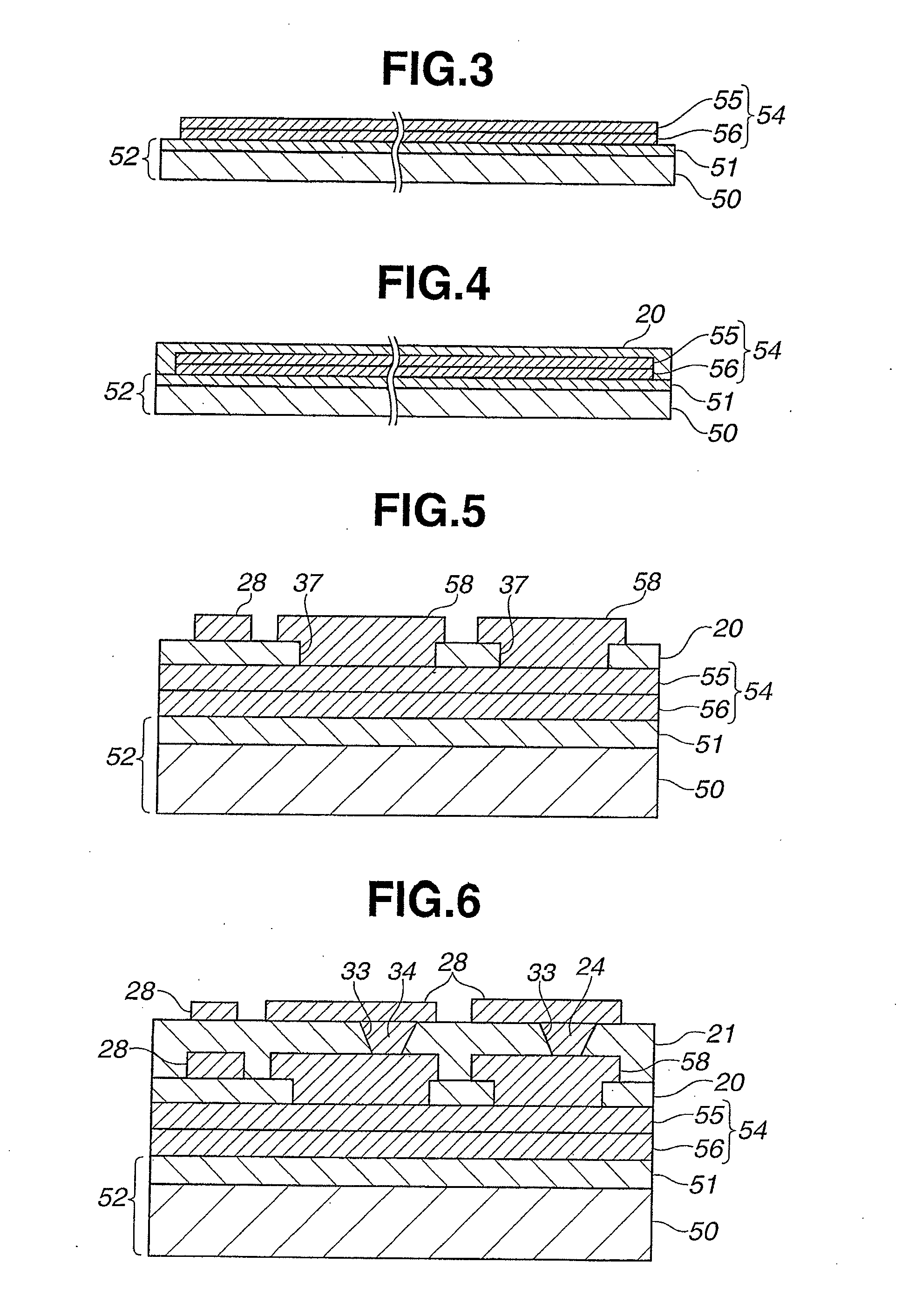
[0156]A fourth preferred embodiment which embodies the second feature according to the present invention will be described in details on a basis of the attached drawings. FIG. 28 is an enlarged cross sectional view representing a rough configuration of the multilayer wiring substrate in the fourth embodiment. In the third embodiment, the coreless wiring substrate formed so as not to include the core substrate is embodied. However, in the fourth embodiment, the present invention embodies the multilayer wiring substrate having the core substrate. The structure and manufacturing method of this multilayer wiring substrate are basically the same as the second embodiment. Hence, only the features different from the second embodiment will be described hereinbelow.

[0157]Recognition marks 71, 72, 73 (refer to FIG. 21) formed according to the difference in the shades of the color of the resin surface are disposed on outermost resin insulating layer 137 exposed at the upper surface side of fir...


PUM

PropertyMeasurementUnit
distanceaaaaaaaaaa
distanceaaaaaaaaaa
thicknessaaaaaaaaaa

Abstract

Disclosed is a method of manufacturing a multilayer wiring substrate having a principal plane of the substrate and a rear plane thereof, having a structure such that a plurality of resin insulating layers and a plurality of conductor layers are laminated, and a plurality of chip component connecting terminals to which chip components are connectable are disposed on the principal plane of the substrate. This method has a feature including a plating layer forming process in which product plating layers which provide the plurality of chip component connecting terminals and a dummy plating layer on the surrounding of the product plating layers are formed on the surface of an exposed outermost resin insulating layer at the principal plane of the substrate. This method permits a thickness dispersion of the chip component connecting terminals to be suppressed and permits a connection reliability thereof to the chip components to be increased.

Description

TECHNICAL FIELD[0001]The present invention relates to a multilayer wiring substrate having a plurality of chip component connecting terminals to which chip components are connectable arranged on a principal plane of the substrate and its manufacturing method.BACKGROUND OF THE INVENTION[0002]In recent years, a semiconductor integrated circuit chip (an IC chip) used as a microprocessor of a computer and so forth has become a higher-speed processing capability and a higher functionality. In this addition, there is a tendency of becoming increased number of terminals and of narrowing inter-terminal pitches in the IC chip. In general, a multiple number of terminals are densely collected and arrayed on a bottom surface of the IC chip. Such a terminal group as described above is connected to a terminal group of a mother board side in a form of a flip-chip. However, since a large difference in the inter-terminal pitch is present between the terminal group of the IC chip and the terminal gro...

Claims


Application Information

Patent Timeline
Patent Type & Authority Applications(United States)
IPC IPC(8): H05K1/11H05K3/10
CPCH05K1/0269Y10T29/49155H05K3/4007H05K3/4602H05K3/4682H05K2201/09781H05K2203/072H05K2203/1105H01L23/49822H01L21/4857H01L21/6835H01L2221/68331H01L2221/68345H01L2221/68381H01L2223/54406H01L2223/5442H01L2223/54426H01L2223/54433H01L2223/54486H01L23/544H01L2224/16225H01L2924/19105H05K1/113
Inventor MAEDA, SHINNOSUKESAIKI, HAJIMEHIRANO, SATOSHI
Owner NGK SPARK PLUG CO LTD
Why Eureka
Try Eureka