

Self-aligned trench contact and local interconnect with replacement gate process
- Summary
- Abstract
- Description
- Claims
- Application Information
AI Technical Summary
Benefits of technology
Problems solved by technology
Method used
Image

Examples
Embodiment Construction
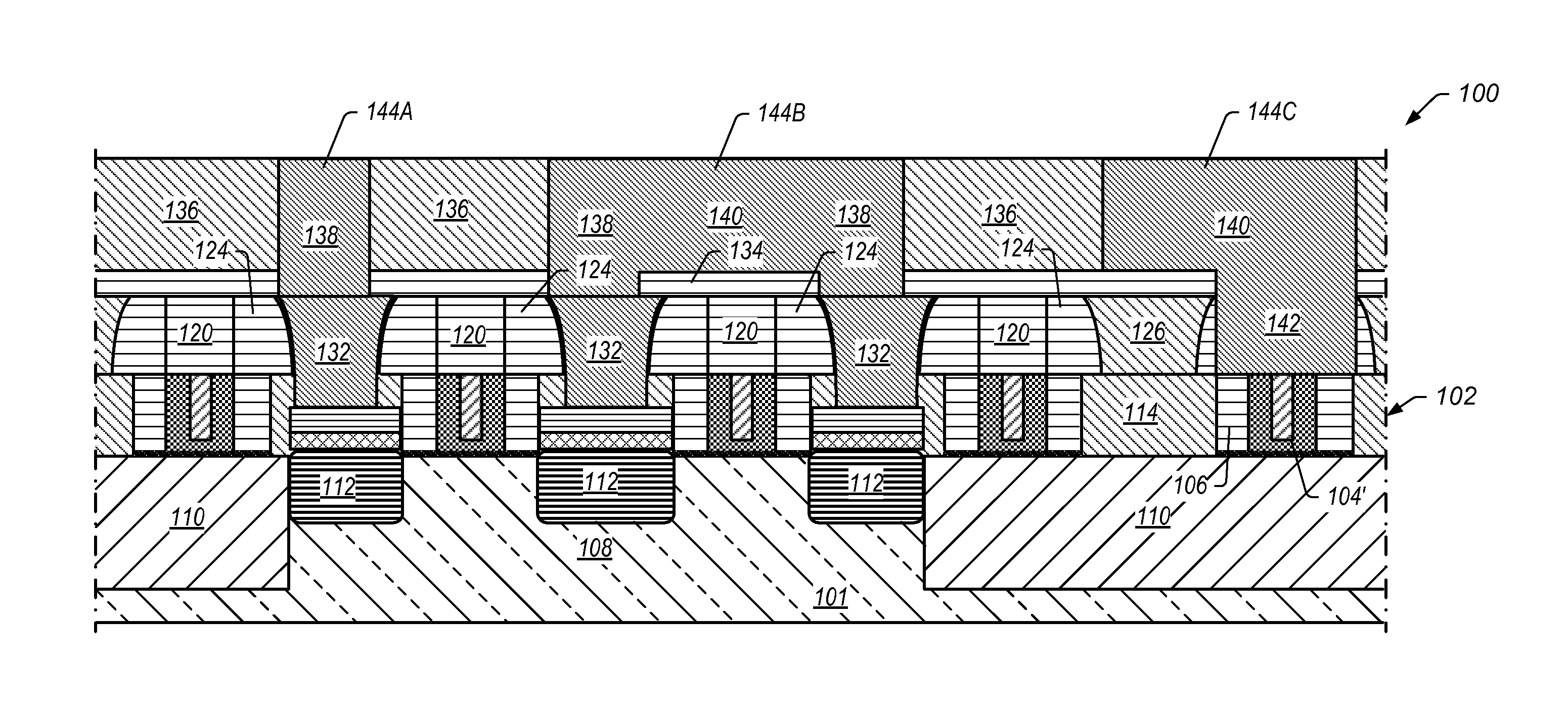
[0013]In certain embodiments, a semiconductor device fabrication process includes providing a transistor with one or more replacement metal gates on a semiconductor substrate. The transistor includes gate spacers of a first insulating material around each gate and a first insulating layer of a second insulating material between the gates and gate spacers. At least some of the second insulating material overlies sources and drains of the gates.
[0014]One or more insulating mandrels are formed and aligned over the gates. The insulating mandrels include the first insulating material. Each insulating mandrel has approximately the same width as its underlying gate with each mandrel being at least as wide as its underlying gate. Mandrel spacers are formed around each insulating mandrel. The mandrel spacers include the first insulating material. Each mandrel spacer has a profile that slopes from being wider at the bottom to narrower at the top.
[0015]A second insulating layer of the second i...
PUM
 Abstract
Description
Claims
Application Information