Polycrystalline silicon efuse and resistor fabrication in a metal replacement gate process

a metal replacement gate and polycrystalline silicon technology, applied in semiconductor devices, semiconductor/solid-state device details, diodes, etc., can solve the problems of increasing challenges in semiconductor integrated circuit processing, presenting compatibility issues with other integrated circuit features, and polycrystalline silicon no longer readily available for efuses

Inactive Publication Date: 2014-01-09
TEXAS INSTR INC
View PDF5 Cites 8 Cited by
  • Summary
  • Abstract
  • Description
  • Claims
  • Application Information

AI Technical Summary

Benefits of technology

[0004]FIGS. 1A through 1I are diagrams of a simplified process flow according to a first embodiment of the present invention;
[0005]FIGS. 2A through 2F and 1G through 1I are diagrams of a simplified process flow according to a second embodiment of the present invention; and
[0006]FIGS. 3A through 3H are diagrams of a simplified process flow according to a third embodiment of the present invention.

Problems solved by technology

Shrinking semiconductor integrated circuit feature sizes have placed increasing challenges on semiconductor integrated circuit processing.
Such advanced processes, however, may present compatibility issues with other integrated circuit features.
With metal gate replacement, however, polycrystalline silicon is no longer readily available for efuses.
Copper efuses, however, have a relatively low resistance and require high current to program or blow them.
Moreover, they present some programming reliability issues regarding incomplete programming and copper leakage contamination.

Method used


Image

  • Polycrystalline silicon efuse and resistor fabrication in a metal replacement gate process
  • Polycrystalline silicon efuse and resistor fabrication in a metal replacement gate process
  • Polycrystalline silicon efuse and resistor fabrication in a metal replacement gate process

Examples


first embodiment

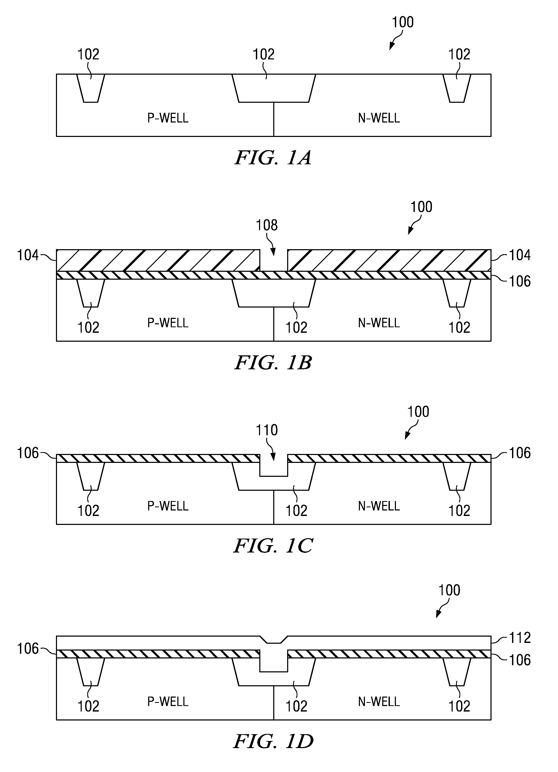
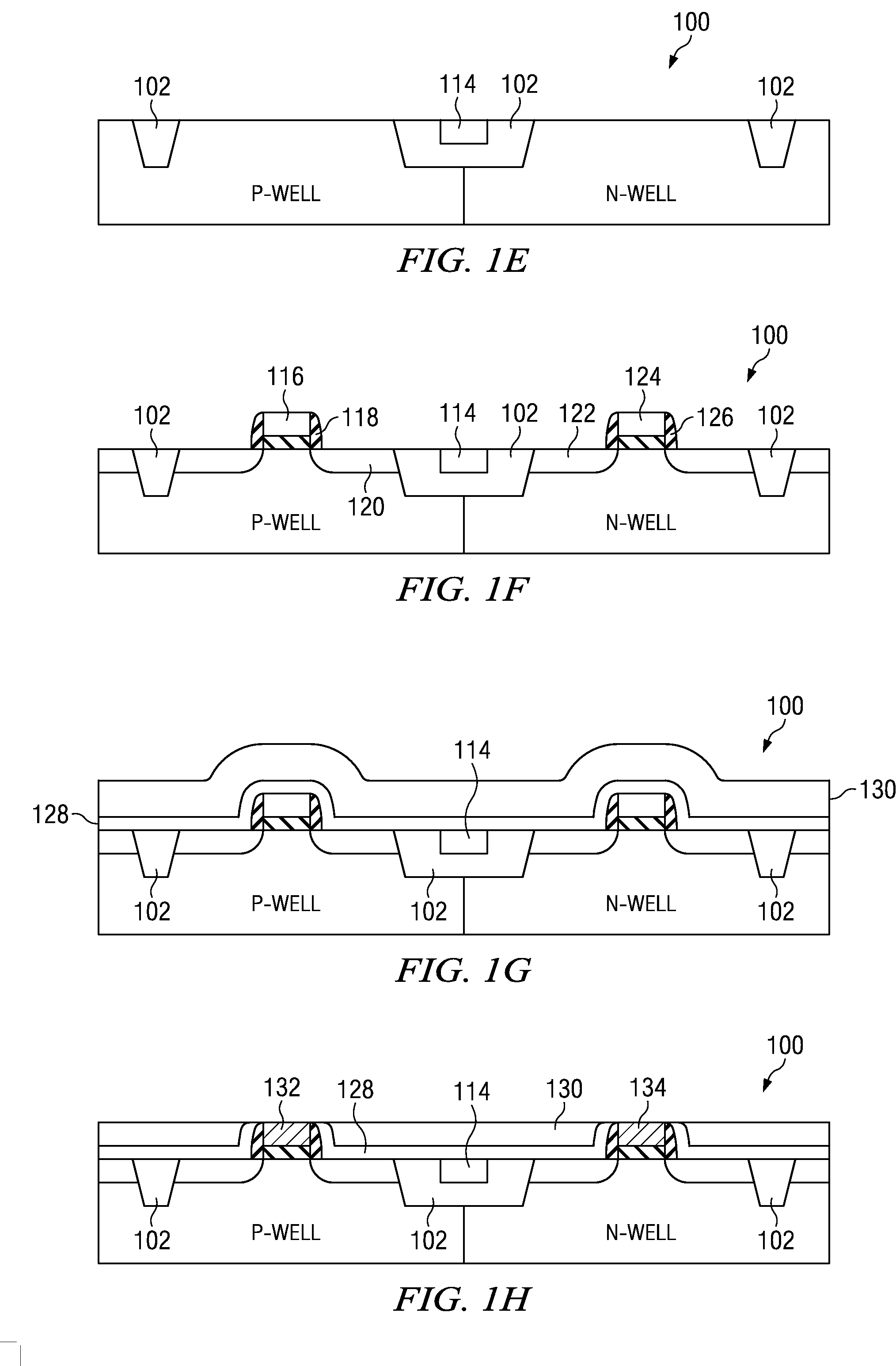
[0008]Referring now to FIGS. 1A through 1I there are diagrams of a simplified process flow according to the present invention. FIG. 1A illustrates a semiconductor substrate 100 having shallow trench isolation (STI) regions 102 as is well known in the art. The left half of the substrate is designated p-well as a bulk terminal for re-channel metal oxide semiconductor (NMOS) transistors. The right half of the substrate is designated n-well as a bulk terminal for p-channel metal oxide semiconductor (PMOS) transistors. Here, and in the following discussion, drawing figures illustrate a simplified fabrication process flow rather than a particular circuit. The drawing figures are not to scale, and the same reference numerals are used to identify similar features.

[0009]At FIG. 1B, a hard mask 106 is formed over the substrate 100 of FIG. 1A. The hard mask is generally an inorganic anti-reflective coating (IARC) and may be silicon nitride (SiN), silicon carbide (SiC), or other suitable materi...

second embodiment

[0017]Referring now to FIGS. 2A through 2F there are diagrams of a simplified process flow according to the present invention. FIG. 2A illustrates a semiconductor substrate 200 having shallow trench isolation (STI) regions 202 as is well known in the art. The left half of the substrate is designated p-well as a bulk terminal for NMOS transistors. The right half of the substrate is designated n-well as a bulk terminal for PMOS transistors.

[0018]At FIG. 2B, a dielectric layer 207 is formed over substrate 200. The dielectric layer may be thermally grown silicon dioxide or a deposited high-k dielectric such as SiON or SiN. Here, high-k refers to a dielectric generally having a relative permittivity greater than 10. A hard mask 206 is formed over the dielectric layer 207 of FIG. 2A. The hard mask is generally an IARC layer as previously described. A photoresist layer 204 is formed over the hard mask 206 layer and opening 208 is patterned in the photoresist layer.

[0019]At FIG. 2C, the har...

third embodiment

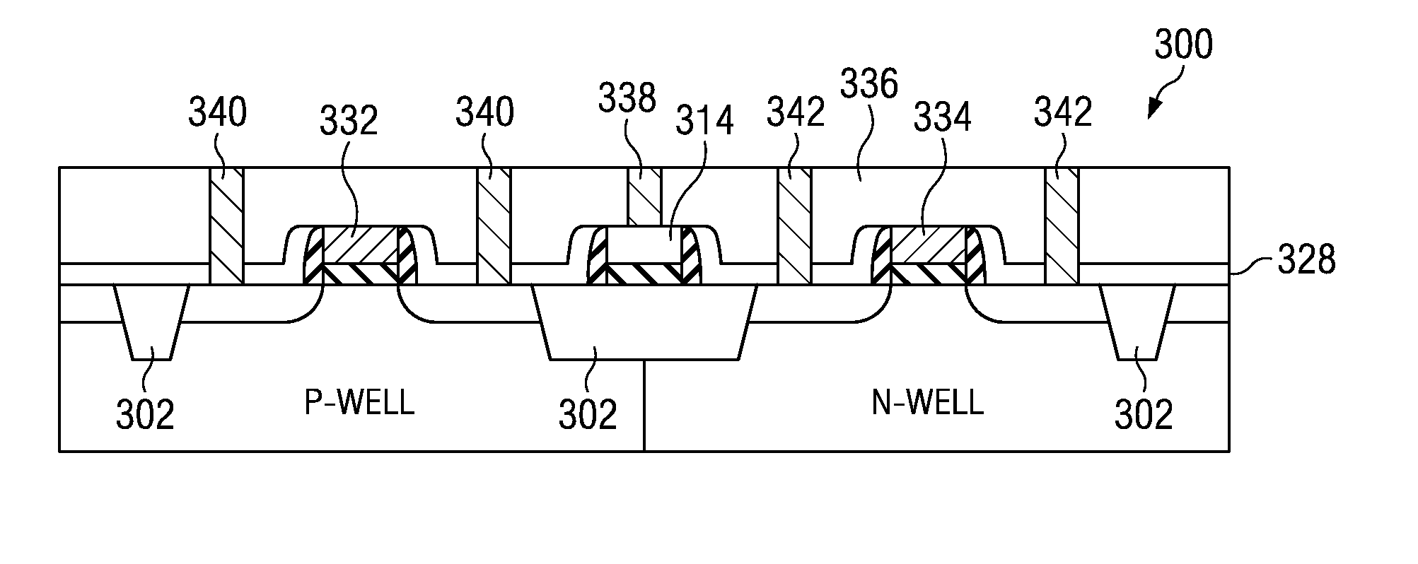
[0024]Referring now to FIGS. 3A through 3H there are diagrams of a simplified process flow according to the present invention. FIG. 3A illustrates a semiconductor substrate 300 having shallow trench isolation (STI) regions 302 as is well known in the art. The left half of the substrate is designated p-well as a bulk terminal for n-channel metal oxide semiconductor (NMOS) transistors. The right half of the substrate is designated n-well as a bulk terminal for p-channel metal oxide semiconductor (PMOS) transistors.

[0025]At FIG. 3B, a dielectric layer 307 is formed over substrate 300. The dielectric layer may be thermally grown silicon dioxide or a deposited high-k dielectric such as SiON or SiN. Here, high-k refers to a dielectric generally having a relative permittivity greater than 10. A conductive layer 312 is formed over the dielectric layer 307. The conductive layer 112 is preferably polycrystalline silicon and may be n-type, p-type, or undoped. A photoresist layer is formed and ...


PUM


Abstract

A method of fabricating an integrated circuit is disclosed (FIGS. 1-2). The method comprises providing a substrate (200) having an isolation region (202) and etching a trench in the isolation region. A first conductive layer (214) is formed within the trench. A first transistor having a first conductivity type (n-channel) is formed at a face of the substrate. The first transistor has a gate (216) formed of the first conductive layer. A second transistor having a second conductivity type (p-channel) is formed at the face of the substrate. The second transistor has a gate (224) formed of the first conductive layer. The method further comprises replacing the first conductive layer of the first transistor with a first metal gate (132) and replacing the first conductive layer of the second transistor with a second metal gate (134).

Description

BACKGROUND OF THE INVENTION[0001]Embodiments of the present invention relate to fabrication of a polycrystalline silicon efuse in a complementary metal oxide semiconductor (CMOS) metal replacement gate process.[0002]Shrinking semiconductor integrated circuit feature sizes have placed increasing challenges on semiconductor integrated circuit processing. In particular, a balance between high packing density and yield requires a finely tuned manufacturing process. Recent process advances include various stress memorization techniques (SMT) in both p-channel and n-channel complementary metal oxide semiconductor (CMOS) circuits, metal gate replacement, and composite gate dielectric materials such as silicon oxynitride (SiON). Such advanced processes, however, may present compatibility issues with other integrated circuit features. Efuses, for example, are used in many integrated circuits for row and column redundancy selection, integrated circuit identification, programmable logic functi...

Claims


Application Information

Patent Timeline
Patent Type & Authority Applications(United States)
IPC IPC(8): H01L21/8238H01L21/28H01L21/02
CPCH01L21/28123H01L21/823842H01L23/5256H01L27/0629H01L28/20H01L29/66545H01L29/78H01L2924/0002H01L2924/00
Inventor MCKEE, BENJAMIN P.JIANG, YONGQIANGGRIDER, DOUGLAS T.
Owner TEXAS INSTR INC
Why Eureka
Try Eureka