Method of preventing stiction of MEMS devices

a technology of microelectromechanical systems and devices, applied in the direction of microelectromechanical systems, semiconductor devices, electrical apparatus, etc., can solve the problems of unintentional contact of surfaces with external environmental forces, increased risk of stiction, and undesirable situation of stiction, so as to prevent stiction

Inactive Publication Date: 2012-12-13
INVENSENSE
View PDF5 Cites 16 Cited by
  • Summary
  • Abstract
  • Description
  • Claims
  • Application Information

AI Technical Summary

Benefits of technology

[0009]Another embodiment of the present invention includes a method comprising providing a TiN contact surface on a substrate for a MEMS structure to prevent stiction between the MEMS structure and the substrate.

Problems solved by technology

Stiction is an undesirable situation which arises when surface adhesion forces are higher than the mechanical restoring force of a MEMS structure.
The greater the contact area at both macroscopic and microscopic roughness levels, the risk of stiction increases.
Surfaces can be unintentionally brought into contact by external environmental forces including vibration, shock and surface tension forces that are present during aqueous sacrificial release steps often used in micro-fabrication processes.
Adherence of the two surfaces may occur causing the undesirable stiction.
Hillock formation on the aluminum surface in CMOS-MEMS devices can prevent proper device operation and is often associated with stress in the aluminum deposited layer.
Elevated temperatures during processing cause metal grains to coalesce into larger grains creating displacements leading to hillock formation and protrusions from the surface.
The use of chemical etchants leads to roughened features on the aluminum surface which may exacerbate the stress induced hillock formation.
Although there is some sensitivity to the hillock formation in standard semiconductor devices, it is more of an issue for MEMS devices where an aluminum surface is a critical feature such as an electrode of a capacitive device on a MEMS structure.

Method used


Image

  • Method of preventing stiction of MEMS devices
  • Method of preventing stiction of MEMS devices
  • Method of preventing stiction of MEMS devices

Examples


Embodiment Construction

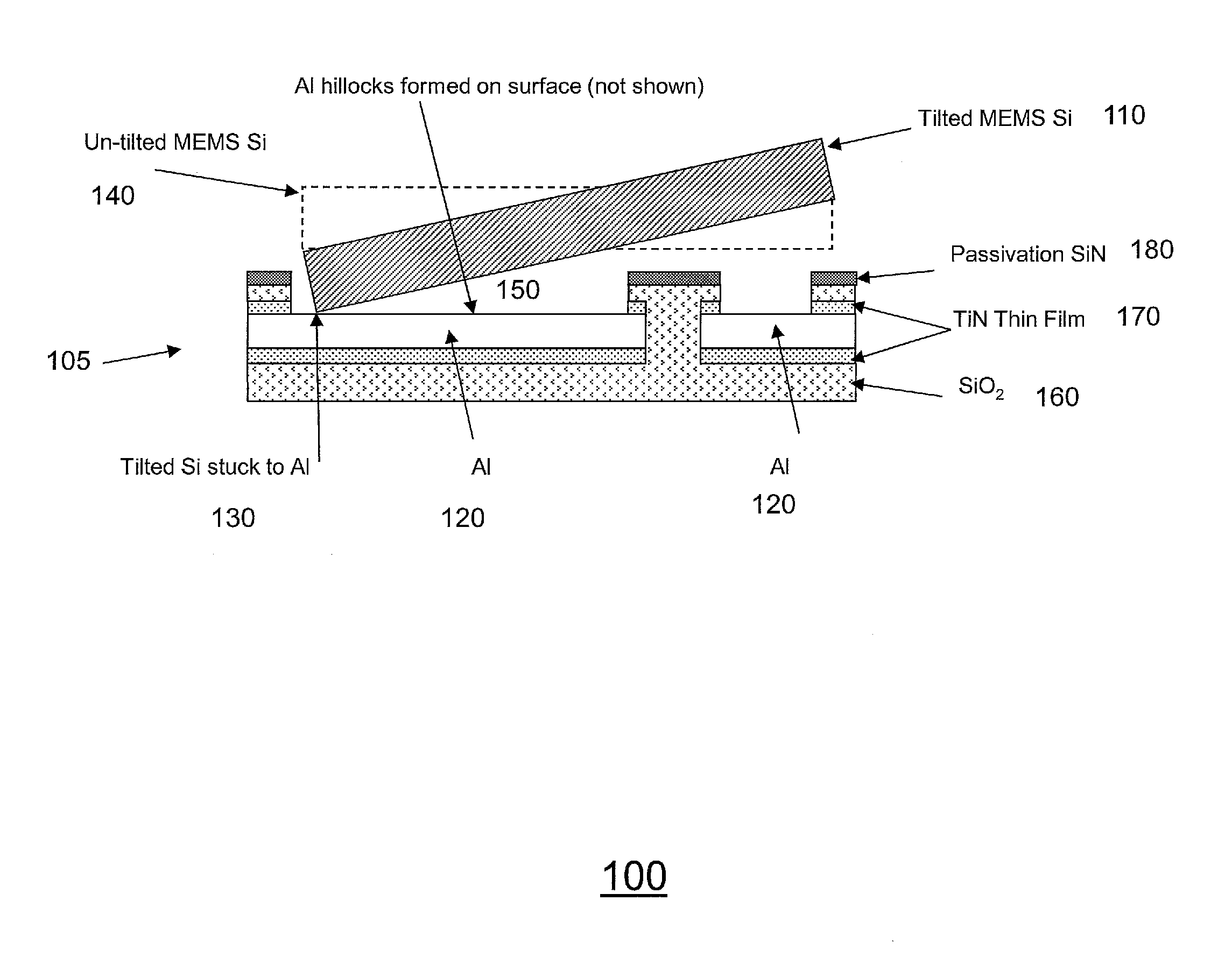
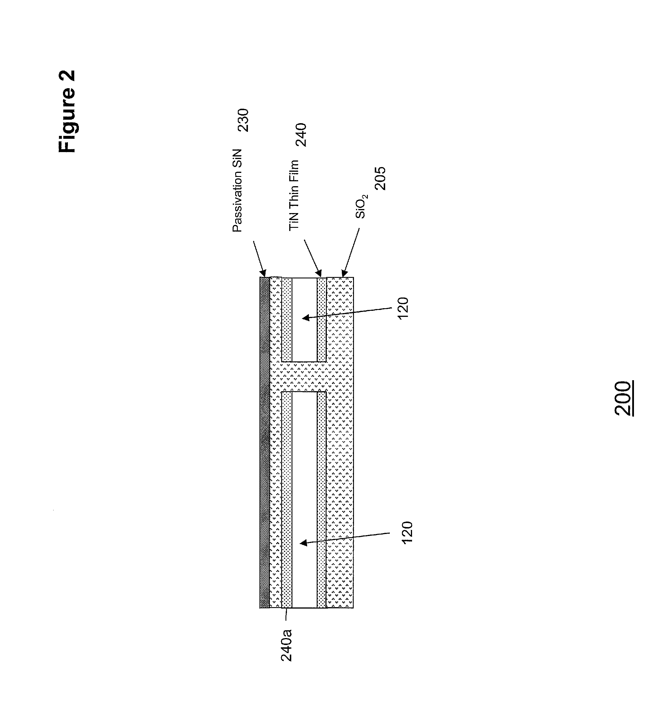
[0018]The present invention relates generally to the fabrication of MEMS devices, and more particularly to reducing the occurrence of stiction and hillock formations in Micro-Electro-Mechanical Systems (MEMS) devices. The present invention provides solutions to reduce or eliminate stiction and hillock formations during MEMS processing.

[0019]The following description is presented to enable one of ordinary skill in the art to make and use the invention and is provided in the context of a patent application and its requirements. Various modifications to embodiments and the generic principles and features described herein will be readily apparent to those skilled in the art. Thus, the present invention is not intended to be limited to the embodiment shown but is to be accorded the widest scope consistent with the principles and features described herein.

[0020]As used herein, the terms stop pads and dimples are intended to be used interchangeably and reflect physical attributes which are...


PUM


Abstract

A method and apparatus are disclosed for reducing stiction in MEMS devices. The method comprises patterning a CMOS wafer to expose Titanium-Nitride (TiN) surface for a MEMS stop and patterning the TiN to form a plurality of stop pads on the top metal aluminum surface of the CMOS wafer. The method is applied for a moveable MEMS structure bonded to a CMOS wafer. The TiN surface and / or plurality of stop pads minimize stiction between the MEMS structure and the CMOS wafer. Further, the TiN film on top of aluminum electrode suppresses the formation of aluminum hillocks which effects the MEMS structure movement.

Description

CROSS-REFERENCE TO RELATED APPLICATION[0001]This application claims the benefit of U.S. Provisional Patent Application No. 61 / 494,766, filed on Jun. 8, 2011, entitled “METHOD OF PREVENTING STICTION OF MEMS DEVICES,” which is incorporated herein by reference in its entirety.FIELD OF THE INVENTION[0002]The present invention relates generally to the fabrication of Micro-Electro-Mechanical Systems (MEMS) devices, and more particularly to reducing the occurrence of stiction of and hillock formation in MEMS devices.BACKGROUND OF THE INVENTION[0003]Fabrication platforms that integrate MEMS structures with electronics may utilize wafer-to-wafer bonding process to directly integrate pre-fabricated MEMS wafers to off-the-shelf CMOS wafers at the wafer level. The process simultaneously provides hermetic sealing of the plurality of devices with electric contacts during the wafer level bonding step.[0004]Stiction is an undesirable situation which arises when surface adhesion forces are higher th...

Claims


Application Information

Patent Timeline
Patent Type & Authority Applications(United States)
IPC IPC(8): H01L29/84H01L21/02
CPCB81B2203/058B81C1/00238B81C2201/112
Inventor HUANG, KEGANGLIM, MARTINLI, XIANG
Owner INVENSENSE
Why Eureka
Try Eureka