Method for forming nitride semiconductor device
a technology of nitride and semiconductors, applied in the field of forming nitride semiconductor devices, can solve the problems of reducing the quality of 2deg, affecting the performance of hemt devices,
- Summary
- Abstract
- Description
- Claims
- Application Information
AI Technical Summary
Benefits of technology
Problems solved by technology
Method used
Image

Examples
first embodiment
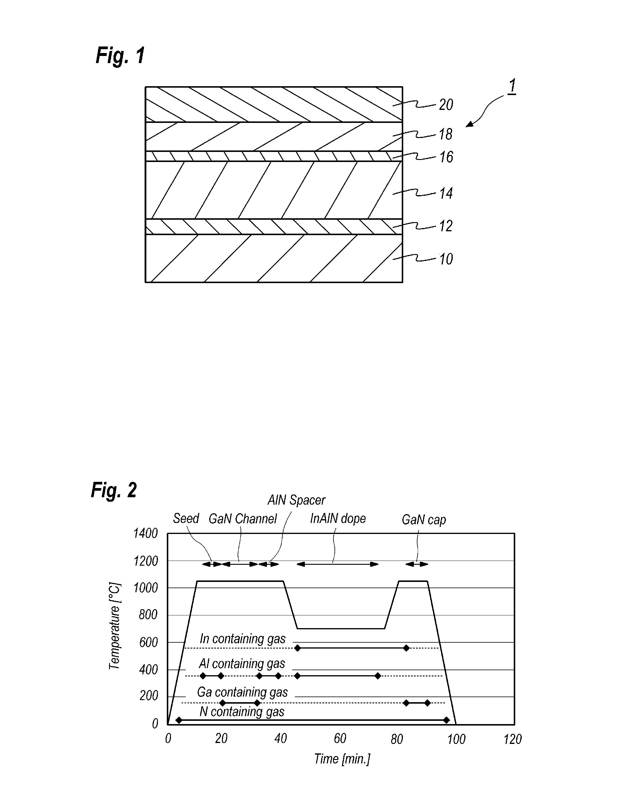
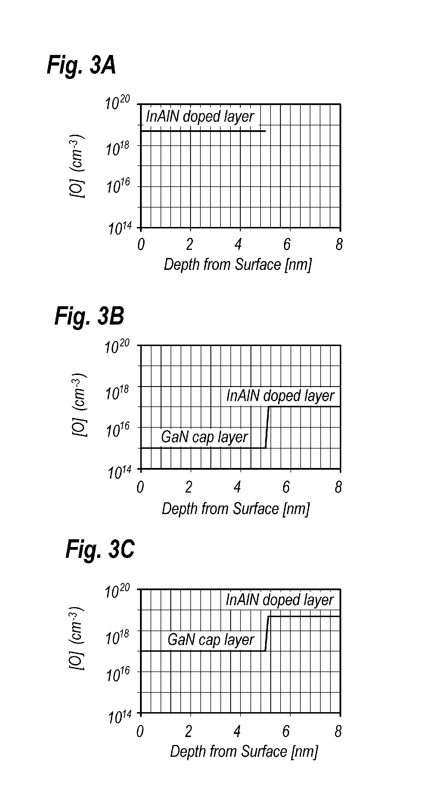
[0023]FIG. 1 shows a cross section of a stack of semiconductor layers applicable to a nitride semiconductor device, and FIG. 2 shows a sequence of a temperature and source materials for the growth of the semiconductor layers shown in FIG. 1. The growth of the semiconductor layers is carried out by the well-known technique of the metal-organized-chemical-vapor-deposition (MOCVD). Referring to FIGS. 1 and 2, the process first sets a substrate 10 made of SiC within a furnace of the MOCVD and converts the interior of the furnace into hydrogen (H) atmosphere. Then, raising the substrate 10 to 1050° C., the process grows a seed layer 12 made of AlN by supplying tri-methyl-aluminum (TMA) and ammonia (NH3) into the growth furnace. A thickness of AlN seed layer 12 may be, for instance, 20 nm.
[0024]Then, keeping the temperature of the substrate 10 in 1050° C., the process grows a channel layer 14 made of GaN on AlN seed layer 12 by supplying tri-methyl-gallium (TMG) and ammonia into the furna...
second embodiment
[0042]Another embodiment of the invention will be described as referring to FIG. 5. The process according to the second embodiment may supply the gas containing not only indium (In) but aluminum (Al) for the period to raise the temperature of the substrate 10. The semiconductor stack applicable to the second embodiment is the same as those shown in FIG. 1. Specifically, the process may grow semiconductor layers from AlN seed layer 12 to AlN spacer layer 16 shown in FIG. 1 on SiC substrate 10 by setting the temperature of SiC substrate 10 to be 1050° C. The conditions to grow those layers are the same as those of the first embodiment.
[0043]Then, the process lowers the temperature down to 700° C. and grows InAlN doped layer 18 under the conditions same as those of the aforementioned embodiment. Continuing the supply of TMI and TMA within the furnace, the process raises the temperature of SiC substrate up to 1050° C. The supply not only TMI but TMA during the rise of the temperature ma...
third embodiment
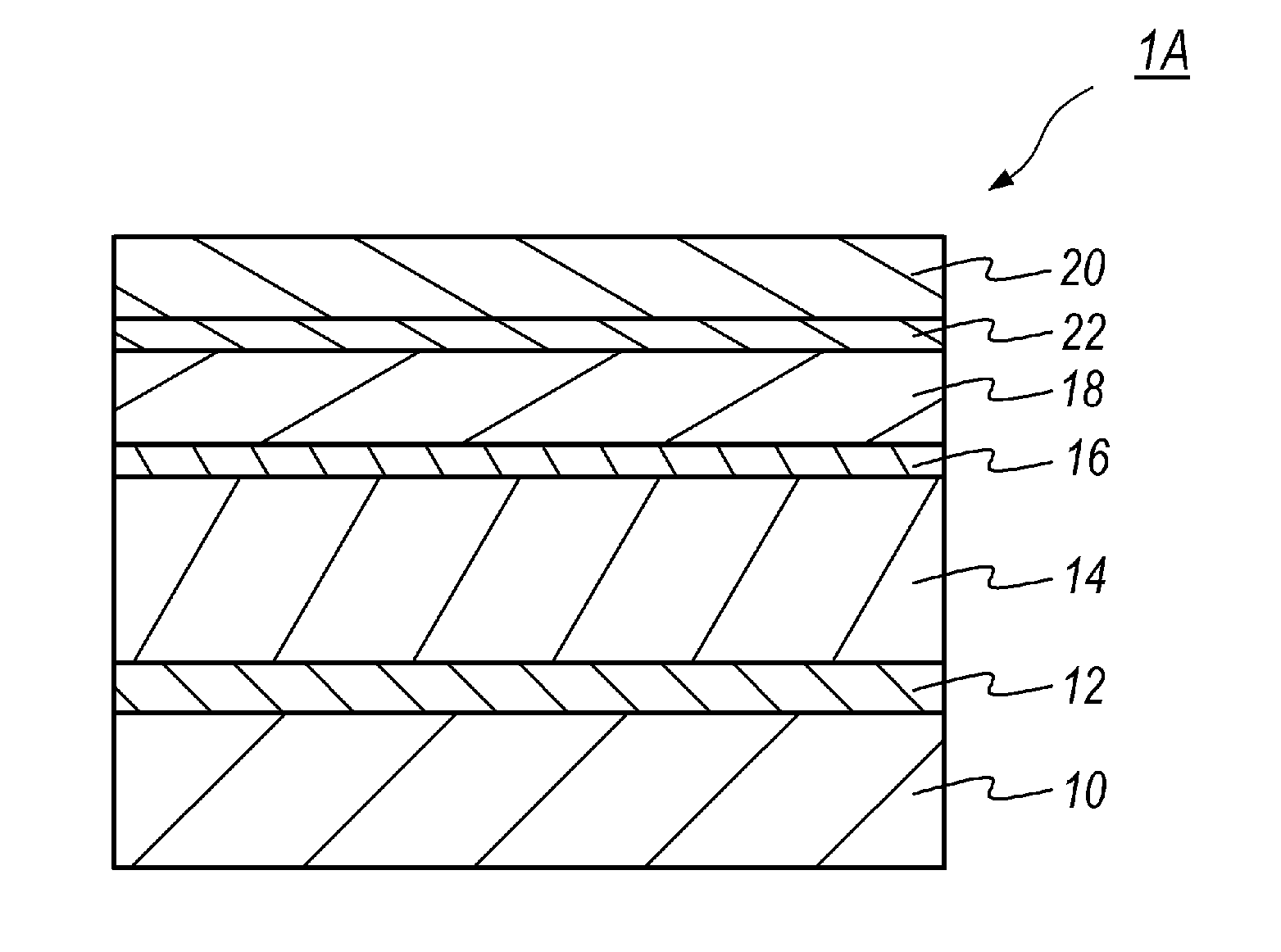
[0052]Still another embodiment according to the present invention will be described as referring to FIG. 6 which shows a cross section of another stack of semiconductor layers according to the third embodiment of the invention. The stack 1A, shown in FIG. 6 has a feature distinguishable from that shown in FIG. 1 in a point that the stack 1A, includes another GaN layer 22 between InAlN doped layer 17 and GaN layer 20. The original GaN cap layer 20 is hereinafter called as the second GaN layer 20, while, additional GaN layer 22 is called as the first GaN layer 22.
[0053]Table 2 below listed summarizes conditions to grow respective layers 12-22 shown in FIG. 6; while FIG. 7 shows a procedure to grow the layers 12-22. Another feature according to the present embodiment is that the conditions to grow two GaN layers, 20 and 22, that is, the present method grows the first GaN layer 22 immediately on InAlN doped layer 18 at a relatively lower temperature of 700° C., which is same with that f...
PUM
| Property | Measurement | Unit |
|---|---|---|
| temperature | aaaaa | aaaaa |
| temperature | aaaaa | aaaaa |
| thickness | aaaaa | aaaaa |
Abstract
Description
Claims
Application Information