Memory controller

a memory controller and controller technology, applied in the field of error correction techniques, can solve the problems of reducing the storage efficiency of information data in a memory, errors in written data in some cases, and errors in stored data, so as to increase the reliability of a semiconductor memory, without complicated data management and operation.

Inactive Publication Date: 2012-12-13
MEGACHIPS
View PDF12 Cites 35 Cited by
  • Summary
  • Abstract
  • Description
  • Claims
  • Application Information

AI Technical Summary

Benefits of technology

[0014]By the present invention, it becomes possible to perform an error correction process on each data without holding information on an error correction mode which is applied to the data.
[0015]Therefore, it is an object of the present invention to increase the reliability of a semiconductor memory whose error rate varies with time, without complicated data management and operation.

Problems solved by technology

When data is written into a nonvolatile semiconductor memory, some errors occur in the written data in some cases.
Further, when data are repeatedly read out from a nonvolatile semiconductor memory, some errors also sometimes occur in stored data.
The decrease in the code rate results in a decrease in storage efficiency of the information data in a memory.
In nonvolatile semiconductor memories, time degradation of cells due to the miniaturization of the process technology is becoming pronounced.
When a nonvolatile semiconductor memory continues to be used, the error rate increases as the cells are degraded.
There is a possibility that the error correcting capability set in an initial state for use may become insufficient with time.
Alternatively, when the error correcting capability is set higher from the beginning of use on the assumption that the cells become degraded with time, the storage efficiency of the information data unnecessarily decreases due to the decrease in the code rate.
Since the code rate is changed, however, the data management and operation becomes complicated.
In other words, since the data length of the code data is changed, the data structure needs to be restructured or the like and the process becomes complicated.

Method used


Image

  • Memory controller
  • Memory controller
  • Memory controller

Examples


Embodiment Construction

The First Preferred Embodiment

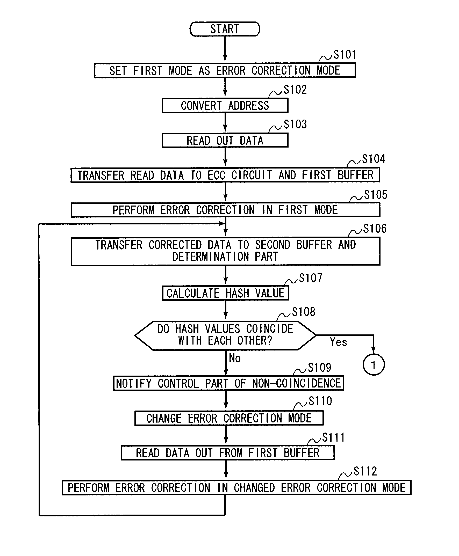
[0028]Hereinafter, with reference to figures, the first preferred embodiment of the present invention will be discussed.

[0029]{1. Overall Structure}

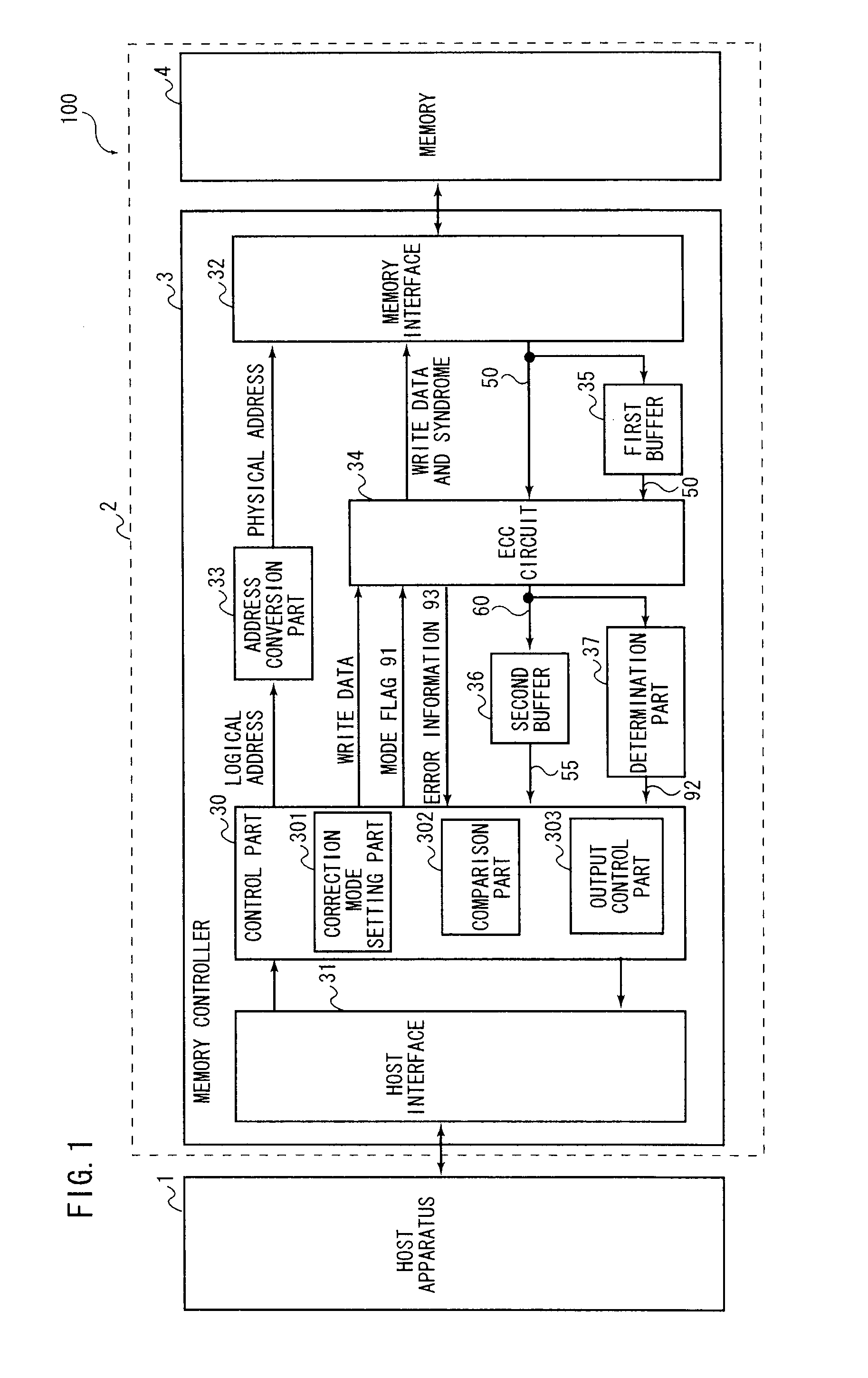
[0030]FIG. 1 is a functional block diagram showing a constitution of an information processing system 100 in accordance with the first preferred embodiment. The information processing system 100 comprises a host apparatus 1 and a memory system 2.

[0031]The host apparatus 1 is, for example, a PC (Personal Computer), a portable terminal, or the like. The memory system 2 is a USB (Universal Serial Bus) memory, a memory card, or the like, which is detachable / attachable from / to the host apparatus 1.

[0032]The memory system 2 comprises a memory controller 3 and a memory 4. The memory controller 3 writes / reads data into / from the memory 4 in response to a request of the host apparatus 1. In other words, the memory controller 3 controls access to the memory 4.

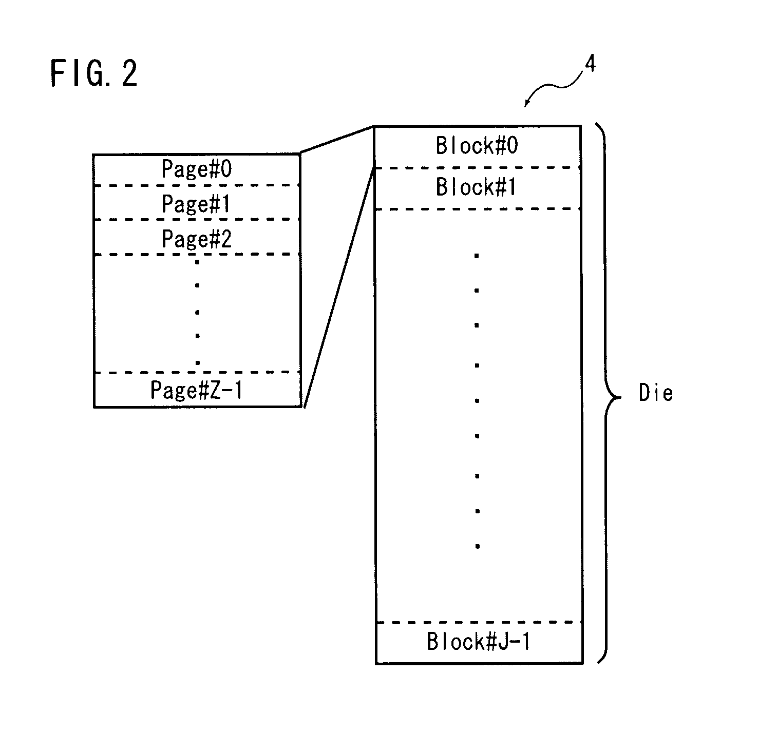
[0033]The memory 4 is a rewritable nonvolatile semiconductor...


PUM


Abstract

An ECC circuit can operate in a plurality of error correction modes with different correcting capabilities for data stored in a memory. The ECC circuit calculates a syndrome with respect to information data in accordance with an error correction mode set by a control part and adds a syndrome of a fixed length in which dummy bits are added to the calculated syndrome, to the information data. When code data is read out, the ECC circuit performs a correction process on the code data by using the syndrome included in the code data.

Description

BACKGROUND OF THE INVENTION[0001]1. Field of the Invention[0002]The present invention relates to an error correction technique for data stored in a semiconductor memory.[0003]2. Description of the Background Art[0004]As recording media for a variety of data, nonvolatile semiconductor memories such as NAND flash memories and the like are widely used. With miniaturization of a process technology or the like, high integration of nonvolatile semiconductor memories is more and more progressing.[0005]When data is written into a nonvolatile semiconductor memory, some errors occur in the written data in some cases. This is a so-called program disturb. Further, when data are repeatedly read out from a nonvolatile semiconductor memory, some errors also sometimes occur in stored data. This is a so-called read disturb. Therefore, for using nonvolatile semiconductor memories including NAND flash memories, it is indispensable to equip the memories with some error correction function.[0006]As circ...

Claims


Application Information

Patent Timeline
Patent Type & Authority Applications(United States)
IPC IPC(8): H03M13/07G06F11/10
CPCG06F11/1048H03M13/05H03M13/3715H03M13/617G06F11/10H03M13/1525H03M13/3738G06F11/1044G11C29/42
Inventor SUGAHARA, TAKAHIKOFUKUSHITA, ERI
Owner MEGACHIPS
Why Eureka
Try Eureka