Method of manufacturing light-emitting device

a technology of light-emitting devices and manufacturing methods, which is applied in the direction of glass making apparatus, glass reforming apparatus, manufacturing tools, etc., can solve the problems of reducing the intensity of bonding of the sealed structure, and affecting the sealing performance of the glass substrate, so as to achieve high reliability and light-emitting devices. high, the effect of excellent hermeticity

Active Publication Date: 2012-12-20
SEMICON ENERGY LAB CO LTD
View PDF7 Cites 63 Cited by
  • Summary
  • Abstract
  • Description
  • Claims
  • Application Information

AI Technical Summary

Benefits of technology

[0039]In accordance with the above method of manufacturing a light-emitting device, the first substrate and the second substrate can be sealed with the glass frit layer forming a closed curve shape. Hence, the light-emitting device can be sealed with the glass frit layer without a break. Thus, a highly reliable light-emitting device can be manufactured.
[0040]In accordance with one embodiment of the present invention, a method of manufacturing a sealed structure with excellent hermeticity can be provided. Alternatively, a method of manufacturing a highly reliable light-emitting device can be provided.

Problems solved by technology

One problem of a method in which a glass frit layer is irradiated with laser light to form a sealed structure is that, when a surface of the glass frit layer is irradiated with laser light, laser light may scatter, which prevents the glass frit layer being completely melted, and accordingly the glass frit layer and the glass substrate may fail to be welded.
A crack generated in the substrate and the glass frit layer serves as a leak path through which an atmospheric component leads to the inside of the sealed structure and impairs sealing performance.
The crack also reduces the intensity of bonding of the sealed structure.

Method used


Image

  • Method of manufacturing light-emitting device
  • Method of manufacturing light-emitting device
  • Method of manufacturing light-emitting device

Examples


embodiment 1

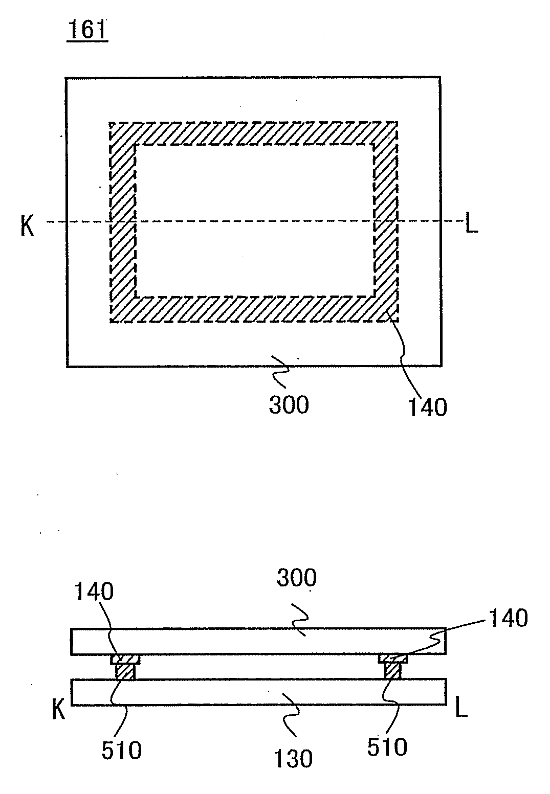
[0062]In this embodiment, the way how a sealed structure 161 illustrated in FIG. 1 is manufactured using a manufacturing method according to one embodiment of the present invention is described with reference to FIGS. 2A to 2C and FIG. 3.

Forming Buffer Layer

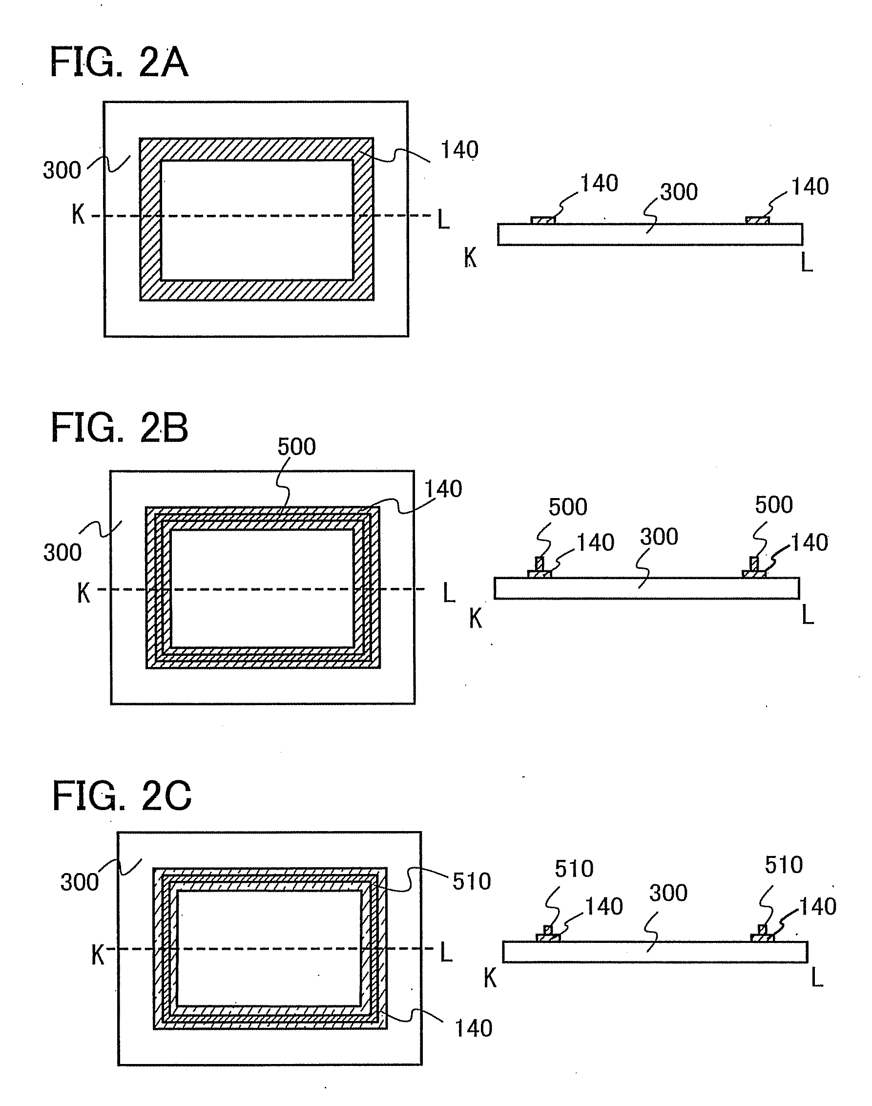
[0063]First, a buffer layer 140 is formed over a second substrate 300. For the second substrate 300, glass is used here, but other materials can be used as long as the second substrate 300 is capable of transmitting laser light because later-described laser light irradiation is performed through the second substrate 300.

[0064]For a film which forms the buffer layer 140, silicon oxide or silicon nitride can be used. A silicon oxide film or a silicon nitride film is formed by a plasma CVD method. In order to reduce a tensile stress generated in the second substrate 300 by the later-described laser light irradiation, the buffer layer 140 has a compressive stress.

[0065]The buffer layer 140 is formed in a region where a glass frit lay...

embodiment 2

[0074]In this embodiment, the way how a sealed structure 162 illustrated in FIG. 4 is manufactured using a manufacturing method according to one embodiment of the present invention is described with reference to FIG. 5 and FIG. 6.

Forming Buffer Layer

[0075]First, a buffer layer 150 is formed over a second substrate 300. For the second substrate 300, glass is used here, but other materials can be used as long as the second substrate 300 is capable of transmitting laser light because the later-described laser light irradiation is performed through the second substrate 300.

[0076]The buffer layer 150 is formed in a region where the glass frit layer 510 is to be formed (FIG. 5). The buffer layer 150 can be formed by a known technique, for example, formed by etching with a resist mask formed using a photomask.

[0077]A film which forms the buffer layer 150 can be formed with a substance which absorbs laser light and has a higher melting point than glass. Specifically, silicon, an insulator s...

embodiment 3

[0093]In this embodiment, one mode of a method of manufacturing a light-emitting device 163 illustrated in FIG. 7 is described with reference to FIGS. 8A and 8B and FIGS. 9A to 9D. In this embodiment, an organic EL element is adapted as one mode of the light-emitting element.

Forming Buffer Layer

[0094]First, the buffer layer 140 is formed over the second substrate 300. For the second substrate 300, although glass is used, other materials can be used as long as the second substrate 300 is capable of transmitting laser light because later-described laser light irradiation is performed through the second substrate 300. The buffer layer 140 is formed in a region where the glass frit layer 510 is to be formed. The buffer layer 140 is formed over the second substrate 300 so that the buffer layer 140 is located to surround the organic EL element 125 when viewed from the top in the state where the second substrate 300 and the first substrate 130 are bonded. The pattern of the buffer layer 14...


PUM

PropertyMeasurementUnit
temperatureaaaaaaaaaa
wavelengthaaaaaaaaaa
thicknessaaaaaaaaaa

Abstract

A method of manufacturing a sealed structure with excellent hermeticity and a method of manufacturing a light-emitting device sealed with the sealed structure. In the methods of manufacturing a sealed structure and a light-emitting device using a glass frit layer, a first step of forming a buffer layer for preventing a crack generated in a substrate and the glass frit layer by laser light irradiation, a second step of forming the glass frit layer to overlap with the buffer layer over the substrate, and a third step of welding the substrates by irradiating the glass frit layer or the buffer layer with laser light are performed, whereby a sealed structure with high hermeticity and a reliable light-emitting device sealed with the sealed structure can be manufactured. By applying the method of manufacturing a light-emitting device especially to an organic EL element, a highly reliable light-emitting device can be obtained.

Description

BACKGROUND OF THE INVENTION[0001]1. Field of the Invention[0002]The present invention relates to a method of manufacturing a sealed structure which can protect an apparatus from impurities from the outside of the device and to a method of manufacturing a light-emitting device.[0003]2. Description of the Related Art[0004]Glass frit sealing is known as a technique of hermetically sealing a space formed by two bonded glass substrates. It is known that a sealed structure using glass frit sealing achieves excellent hermeticity, and such a sealed structure has been applied to electroluminescent (hereinafter abbreviated as EL) display devices, liquid crystal display devices, plasma display devices, and the like.[0005]Attempts have been made to apply glass frit sealing particularly to EL display devices, expecting reliability improvement of EL elements. In organic EL elements, an organic EL layer or electrodes between which the organic EL layer is provided may rapidly decrease in reliabilit...

Claims


Application Information

Patent Timeline
Patent Type & Authority Applications(United States)
IPC IPC(8): C03B23/203
CPCC03C27/06
Inventor SHIMOMURA, AKIHISA
Owner SEMICON ENERGY LAB CO LTD
Why Eureka
Try Eureka