Contact for silicon heterojunction solar cells

a silicon heterojunction, solar cell technology, applied in the direction of semiconductor devices, electrical devices, nanotechnology, etc., can solve the problem of low doping efficiency and achieve the effect of increasing the band offset with the substrate and effectively increasing the doping level over a single material conta

Inactive Publication Date: 2012-12-20
IBM CORP
View PDF3 Cites 52 Cited by
  • Summary
  • Abstract
  • Description
  • Claims
  • Application Information

AI Technical Summary

Benefits of technology

[0008]A photovoltaic device and method include a substrate coupled to an emitter side structure on a first side of the substrate and a back side structure on a side opposite the first side of the substrate. The emitter side structure or the back side structure include layers alternating between wide band gap layers and narrow band gap layers to provide

Problems solved by technology

In addition, the issue of low doping effi

Method used


Image

  • Contact for silicon heterojunction solar cells
  • Contact for silicon heterojunction solar cells
  • Contact for silicon heterojunction solar cells

Examples


Embodiment Construction

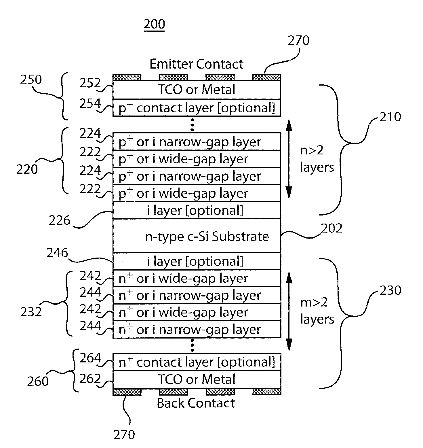
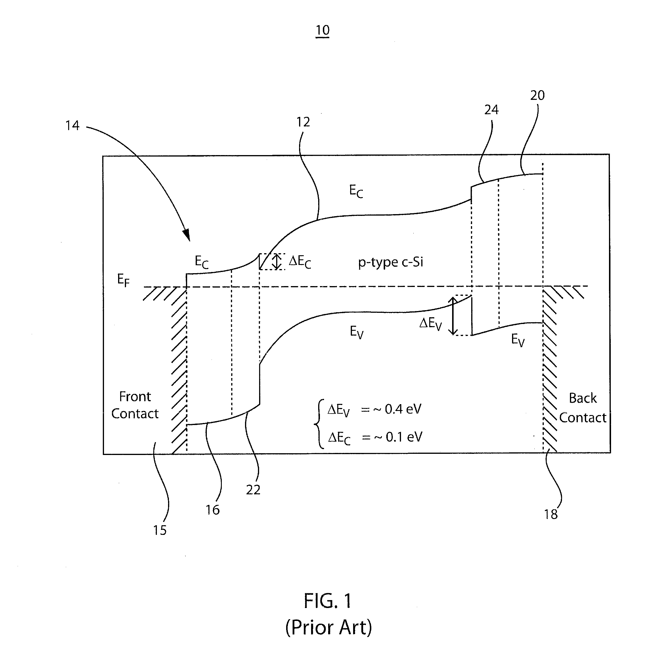
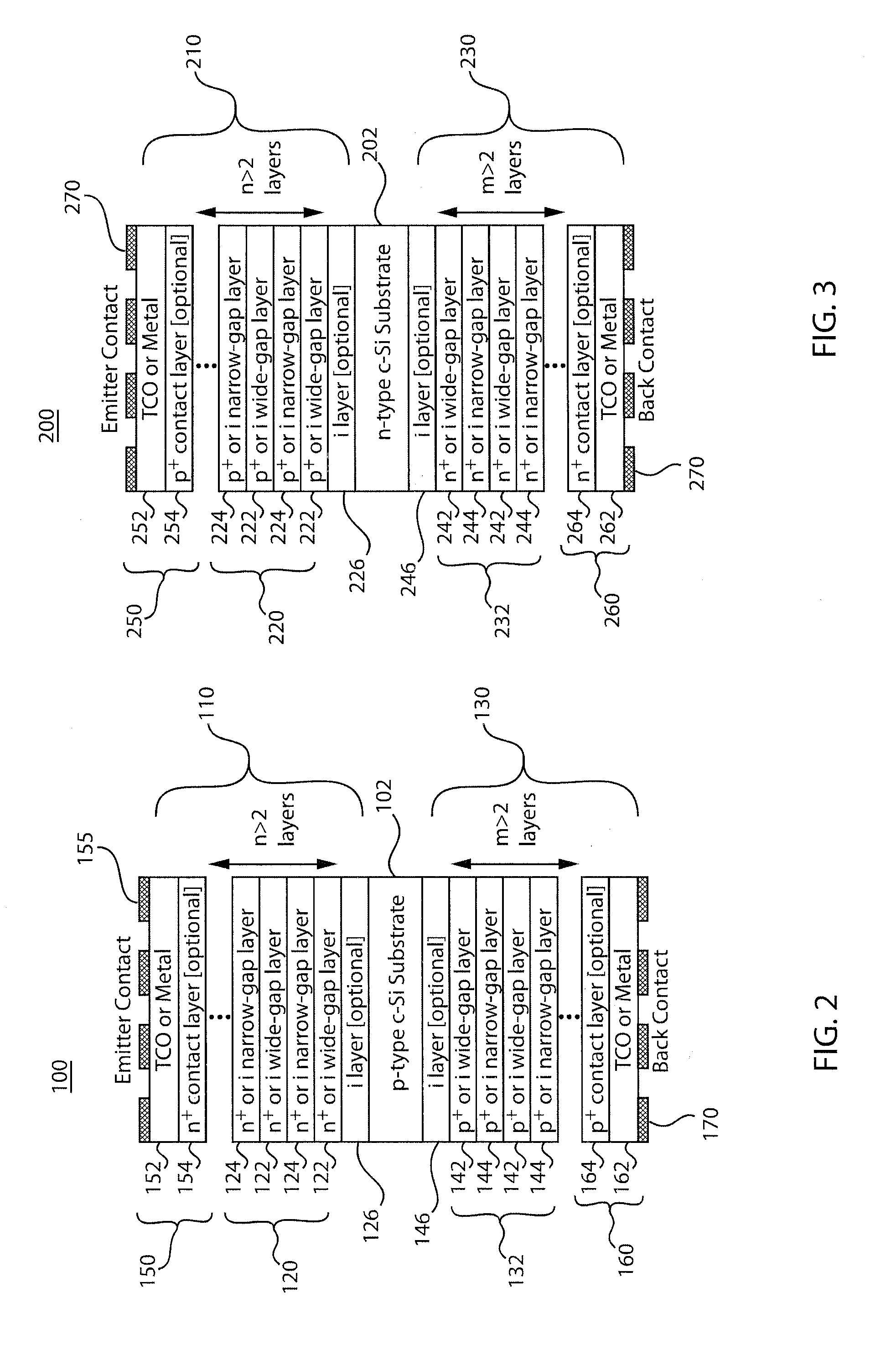
[0020]In accordance with the present principles, superlattice contact structures and methods for forming the same are provided for heterojunction solar cells. The superlattice structure improves open circuit voltage of the cell without compromising fill factor (FF). The open-circuit voltage is improved due to a larger effective band-offset of the superlattice contact and / or modulation (transfer) doping of a low band gap material in the superlattice without pinning the Fermi level. For example, n-type doping may be enhanced by the transfer of electrons from the wide bandgap material to the narrow band gap material or the transfer of holes from the narrow bandgap material to the wide band gap material. Likewise, p-type doping may be enhanced by the transfer of holes from the wide bandgap material to the narrow band gap material or the transfer of electrons from the narrow bandgap material to the wide band gap material. The fill factor is not compromised by overall reduced thickness of...


PUM


Abstract

A photovoltaic device and method include a substrate coupled to an emitter side structure on a first side of the substrate and a back side structure on a side opposite the first side of the substrate. The emitter side structure or the back side structure include layers alternating between wide band gap layers and narrow band gap layers to provide a multilayer contact with an effectively increased band offset with the substrate and/or an effectively higher doping level over a single material contact. An emitter contact is coupled to the emitter side structure on a light collecting end portion of the device. A back contact is coupled to the back side structure opposite the light collecting end portion.

Description

BACKGROUND[0001]1. Technical Field[0002]The present invention relates to photovoltaic devices, and more particularly to contact structures which improve performance of heterojunction cells.[0003]2. Description of the Related Art[0004]Heterojunction with intrinsic thin layer (HIT) solar cells have improved in efficiency (e.g., 23% efficiency in the laboratory and 21% efficiency in production). The HIT cells are comprised of intrinsic / doped hydrogenated amorphous silicon (a-Si:H) serving as front (emitter) and back contacts, on a crystalline silicon (c-Si) absorber with p-type or n-type doping. An advantage of HIT cells is the low deposition temperature of a-Si:H (˜200° C.) which offers a lower thermal budget as compared to conventional c-Si cell processes (˜1000° C.). The low process temperature also permits the use of low-cost Si wafers by preserving carrier lifetime.[0005]Referring to FIG. 1, an energy band diagram of a conventional HIT cell 10 on a p-type crystalline silicon (c-Si...

Claims


Application Information

Patent Timeline
IPC IPC(8): H01L31/06H01L31/20
CPCH01L31/035236B82Y20/00H01L31/0747Y02E10/50Y02E10/547H01L31/022441H01L31/035254H01L31/0516
Inventor HEKMATSHOAR-TABARI, BAHMANSADANA, DEVENDRA K.SHAHIDI, GHAVAM G.SHAHRJERDI, DAVOOD
Owner IBM CORP
Why Eureka
Try Eureka