HEMT including ain buffer layer with large unevenness

Inactive Publication Date: 2012-12-27
SUMITOMO ELECTRIC IND LTD
View PDF2 Cites 7 Cited by
  • Summary
  • Abstract
  • Description
  • Claims
  • Application Information

AI Technical Summary

Benefits of technology

[0009]Because the buffer layer of the embodiment inherently has a portion with smaller thickness, the buffer layer may accelerate carriers captured

Problems solved by technology

However, electrons introduced in 2DEG are sometimes captured in traps caused in the nitride semicon

Method used


Image

  • HEMT including ain buffer layer with large unevenness
  • HEMT including ain buffer layer with large unevenness
  • HEMT including ain buffer layer with large unevenness

Examples


first embodiment

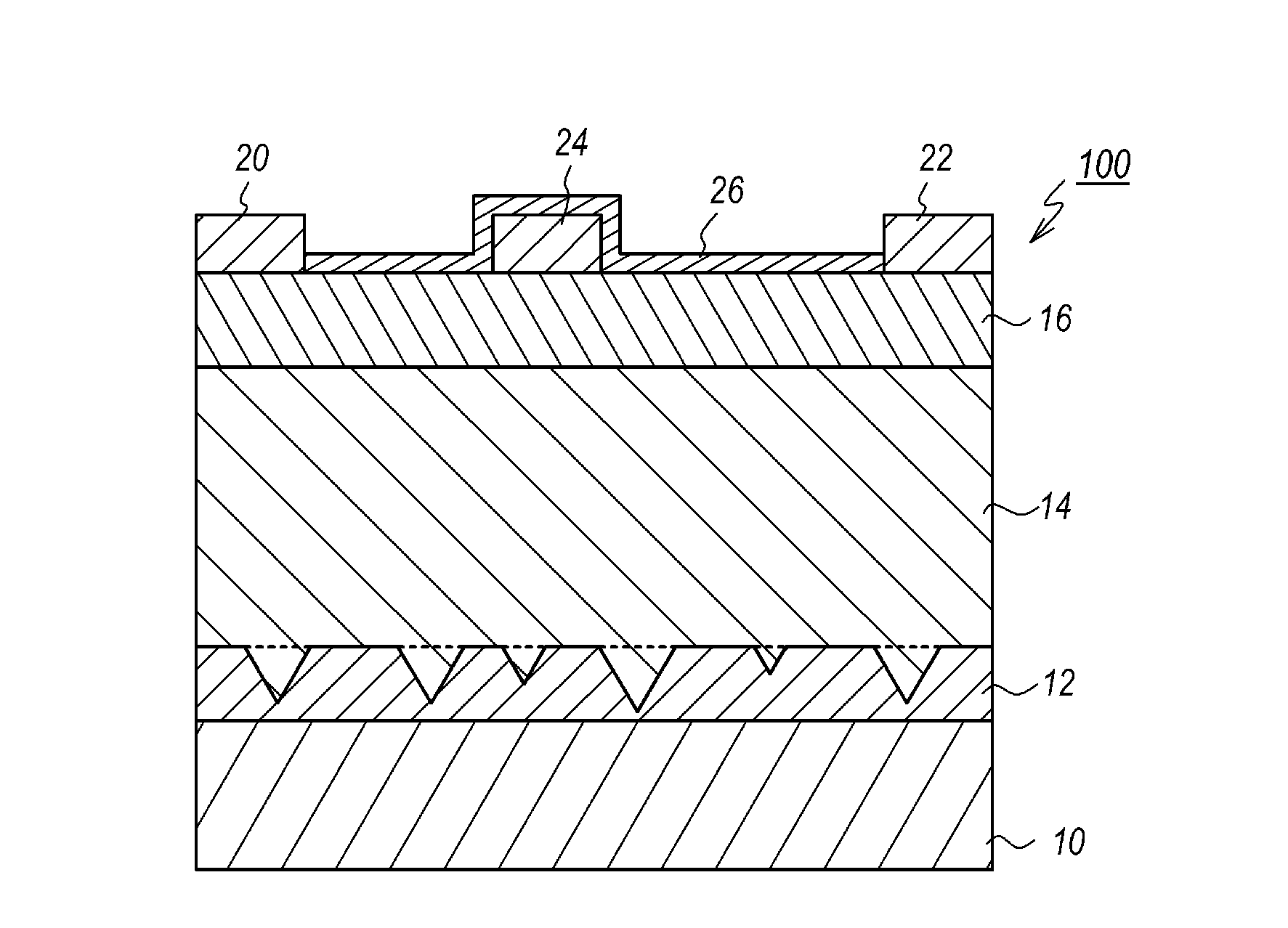
[0029]FIG. 3A shows a cross section of a HEMT according to the first embodiment of the invention. Arrangements of the HEMT 100 shown in FIG. 3A same as those shown in FIG. 1 will be omitted in their explanations. The HEMT 100 includes a substrate 10, a buffer layer 12, a channel layer 14, a doped layer 16, electrodes of the source 20, the drain 22, and the gate 24, and a protection film 26, each layers and electrodes are stacked on the substrate 10 in this order.

[0030]Specifically, the buffer layer 12 is provided on the substrate 10, the channel layer 14 is stacked on the buffer layer 12, the doped layer 16 is stacked on the channel layer 14; and the electrodes, 20 to 24, are provided on the doped layer 16. Moreover, the buffer layer 12 may be made of aluminum nitride (AlN) and has an uneven top surface. FIG. 3A schematically illustrates the unevenness of the top of the buffer layer 12, whose depths and counts are schematically appeared only for the explanations. A feature of the HE...


PUM


Abstract

A HEMT comprised of nitride semiconductor materials is disclosed. The HEMT includes, on a SiC substrate, a AlN buffer layer, a GaN channel layer, and a AlGaN doped layer. A feature of the HEMT is that the AlN buffer layer is grown on an extraordinary condition of the pressure, and has a large unevenness in a thickness thereof to enhance the release of carriers captured in traps in the substrate back to the channel layer.

Description

BACKGROUND OF THE INVENTION[0001]1. Field of the Invention[0002]The present invention relates to a semiconductor device, in particular, the invention relates to a semiconductor device made of primarily nitride material.[0003]2. Related Background Arts[0004]A nitride semiconductor has been practically applied in a high-frequency device as a type of, what is called, a high electron mobility transistor (HEMT). A HEMT generally forms a two-dimensional electron gas (2DEG) introduced in the channel layer at the interface against the doped layer, and 2DEG may operate as carriers in the HEMT. However, electrons introduced in 2DEG are sometimes captured in traps caused in the nitride semiconductor material, which reduces the current flowing in the HEMT and degrades the performance thereof. One prior art, Japanese Patent Application published as JP-2006-147663A, has disclosed a technique to suppress the reduction of the current by enhancing the crystal quality of gallium nitride (GaN).SUMMARY...

Claims


Application Information

Patent Timeline
IPC IPC(8): H01L29/778H01L21/20
CPCH01L21/02378H01L21/02458H01L21/02494H01L21/02502H01L29/2003H01L21/0262H01L29/66462H01L29/7783H01L29/7787H01L21/0254
Inventor NAKATA, KENYUI, KEIICHI
Owner SUMITOMO ELECTRIC IND LTD
Why Eureka
Try Eureka