Methods for cmos-mems integrated devices with multiple sealed cavities maintained at various pressures

a technology of cmos and mems, applied in the field of mems devices, can solve problems such as failure to overcome challenges, and achieve the effect of greater flexibility

Active Publication Date: 2012-12-27
INVENSENSE
View PDF6 Cites 220 Cited by
  • Summary
  • Abstract
  • Description
  • Claims
  • Application Information

AI Technical Summary

Benefits of technology

[0013]A further embodiment of the present invention (Approach D) provides for a method for integrating a secondary sealed enclosure in parallel with a main sealed enclosure. The pressure and ambient gas in the main enclosure is determined during wafer bonding process and the pressure in the secondary sealed enclosure is determined by a post bond sealing of a designed breach or channel of the second enclosure. The post bond process will expose the enclosure to the appropriate pressure and then seal it at that pressure. Each enclosure initially has approximately the same pressure, comprising the steps of: processing a wafer using the Nasiri Fabrication process to create one or more pressure ports. A controlled breach is then created in the second enclosure, and the wafer is then sealed in an ambient that is desirable for the second enclosure. The sealing process operating pressure defines the pressure of the second enclosure. An extension of this embodiment is to design the port to comprise a channel having a gas flow resistance between the port and a secondary enclosure. The flow resistance provides a slow conductance path for a gas to flow into or out of the enclosure. The conductance is then a function of the pressure differential which can be applied in a step separate from the final sealing step. The resistance path is designed to be conductive or flowable for a larger pressure differential but can be relatively non-flowing at pressure differentials less than one atmosphere. A high pressure source is envisioned to provide the necessary pressure differential to push desired gas into or out of the secondary enclosure. Alternately, a sufficiently long exposure at a lower pressure differential may be sufficient to achieve the desired pressure inside the second enclosure. This provides a greater flexibility of pressure values for the second enclosure where the pressure and ambient gas are not dependent on the sealing process.

Problems solved by technology

Unfortunately, these attempts do not overcome the challenges encountered when integrating multiple MEMS devices on a single chip, where it is often desirable to have different devices sealed at different pressures involving minimal processing steps, achieving a more predictable outcome through improved control, and having reduced requirements for the commodity of space or “real estate.” Similarly, what is desired is a system and method that overcomes these challenges and provides for two or more cavities with different pressures or requiring different ambient gasses for operation on the same chip involving a wafer bonding technique.

Method used


Image

  • Methods for cmos-mems integrated devices with multiple sealed cavities maintained at various pressures
  • Methods for cmos-mems integrated devices with multiple sealed cavities maintained at various pressures
  • Methods for cmos-mems integrated devices with multiple sealed cavities maintained at various pressures

Examples


Embodiment Construction

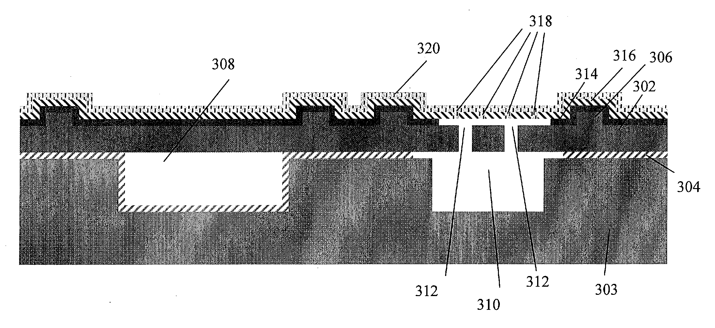
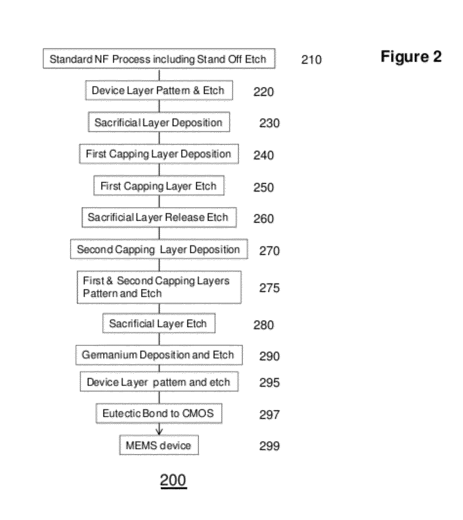
[0059]The present invention relates generally to the fabrication of MEMS devices, and more particularly to providing for two or more cavities with different pressures, or requiring different ambient gasses for operation, on the same chip involving a wafer bonding technique. The present invention provides for multiple approaches and methods for creating multiple pressure levels in multiple cavities fabricated on the chip by a process such as an NF process.

Approach Comparisons

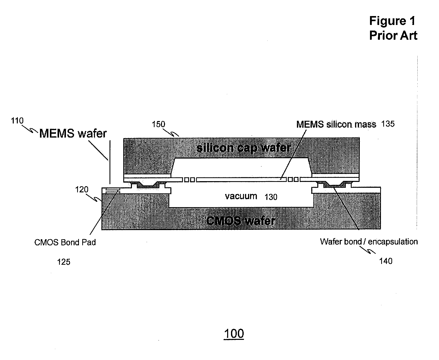
[0060]The present invention relates generally to MEMS devices and more particularly relates to MEMS devices that are hermetically sealed. Presented are four methods, which are described below and include: A. Secondary sealed enclosure, B. Multiple ambient enclosures created during wafer bonding (with four approaches), C. Internal gas reservoir, and D. Controlled leak / breach (with three approaches). Table 1 presents a generalized summary of the advantages of each method and approach.

TABLE 1Comparison of several ap...


PUM


Abstract

A Microelectromechanical systems (MEMS) structure comprises a MEMS wafer. A MEMS wafer includes a handle wafer with cavities bonded to a device wafer through a dielectric layer disposed between the handle and device wafers. The MEMS wafer also includes a moveable portion of the device wafer suspended over a cavity in the handle wafer. Four methods are described to create two or more enclosures having multiple gas pressure or compositions on a single substrate including, each enclosure containing a moveable portion. The methods include: A. Forming a secondary sealed enclosure, B. Creating multiple ambient enclosures during wafer bonding, C. Creating and breaching an internal gas reservoir, and D. Forming and subsequently sealing a controlled leak/breach into the enclosure.

Description

CROSS-REFERENCE TO RELATED APPLICATION[0001]This application claims the benefit of U.S. Provisional Patent Application No. 61 / 501,652, filed on Jun. 27, 2011, entitled “MEMS DEVICES, INTEGRATED MEMS-CMOS,” which is incorporated herein by reference in its entirety.FIELD OF THE INVENTION[0002]The present invention relates generally to MEMS (Microelectromechanical systems) devices and more particularly relates to MEMS devices that are hermetically sealed.BACKGROUND OF THE INVENTION[0003]MEMS technology has advanced to provide integrated packaging of the MEMS devices or sensors. This integration advancement typically refers to processes or methods at which the packaging of the MEMS device is in the form of a protective cap which hermetically seals the device from the outside environment. Furthermore it protects the MEMS device from subsequent assembly operations such as saw cutting for singulation. The processes and methods are performed at a wafer level rather than a die level. The waf...

Claims


Application Information

Patent Timeline
Patent Type & Authority Applications(United States)
IPC IPC(8): H01L29/84H01L21/02
CPCB81B7/02B81C2203/019B81C2203/0145B81C1/0023B81C1/00293
Inventor DANEMAN, MICHAELLIM, MARTINHUANG, KEGANGTCHERTKOV, IGOR
Owner INVENSENSE
Why Eureka
Try Eureka