Memory Architecture of 3D Array With Diode in Memory String

a memory string and memory technology, applied in the field of memory architecture of 3d arrays with diodes in memory strings, can solve the problems of limiting the use of technology, limiting the number of control gates that can be layered in this way, and high manufacturing costs

Inactive Publication Date: 2012-12-27
MACRONIX INT CO LTD
View PDF19 Cites 76 Cited by
  • Summary
  • Abstract
  • Description
  • Claims
  • Application Information

AI Technical Summary

Benefits of technology

[0012]Diodes positioned by the source line end of the NAND string perform electrical isolation between the source line end of the NAND string and the source line. With the diodes performing such electrical isolation, the GSL ground select line-controlled transistors are not required to selectively isolate the source line end of the NAND string from the source line.

Problems solved by technology

So, although the benefits of higher density are achieved using 3D arrays, the higher manufacturing costs limit the use of the technology.
Also, there is a limit in the number of control gates that can be layered in this way, determined by such factors as the conductivity of the vertical channel, program and erase processes that are used and so on.

Method used


Image

  • Memory Architecture of 3D Array With Diode in Memory String
  • Memory Architecture of 3D Array With Diode in Memory String
  • Memory Architecture of 3D Array With Diode in Memory String

Examples


Embodiment Construction

[0099]A detailed description of embodiments is provided with reference to the Figures.

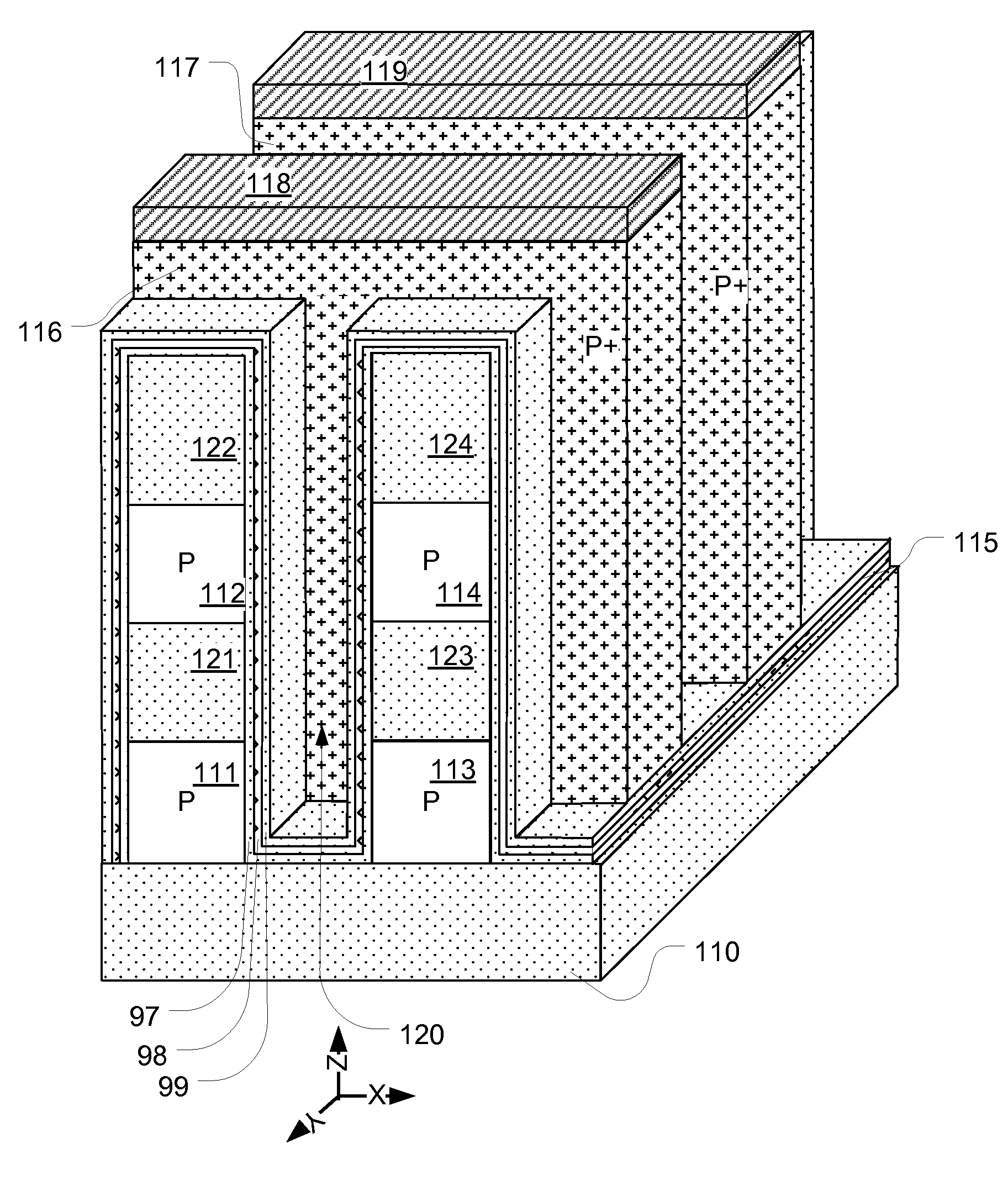
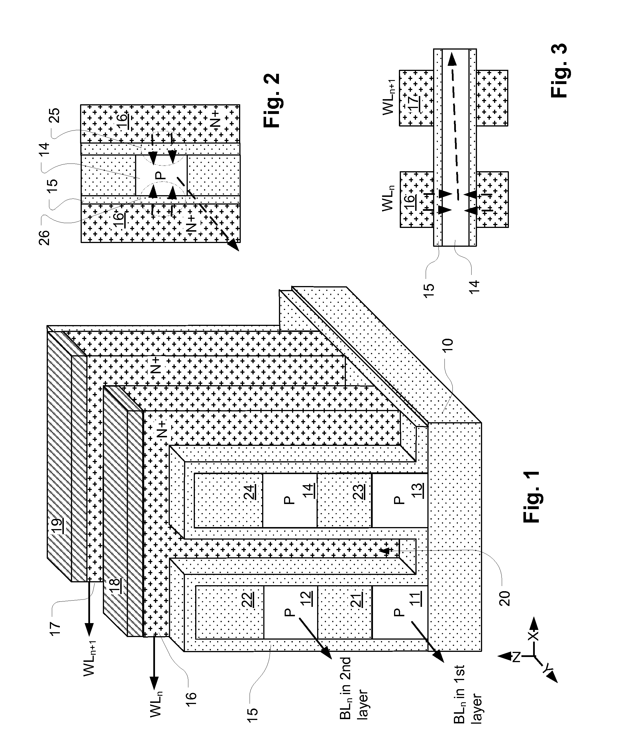
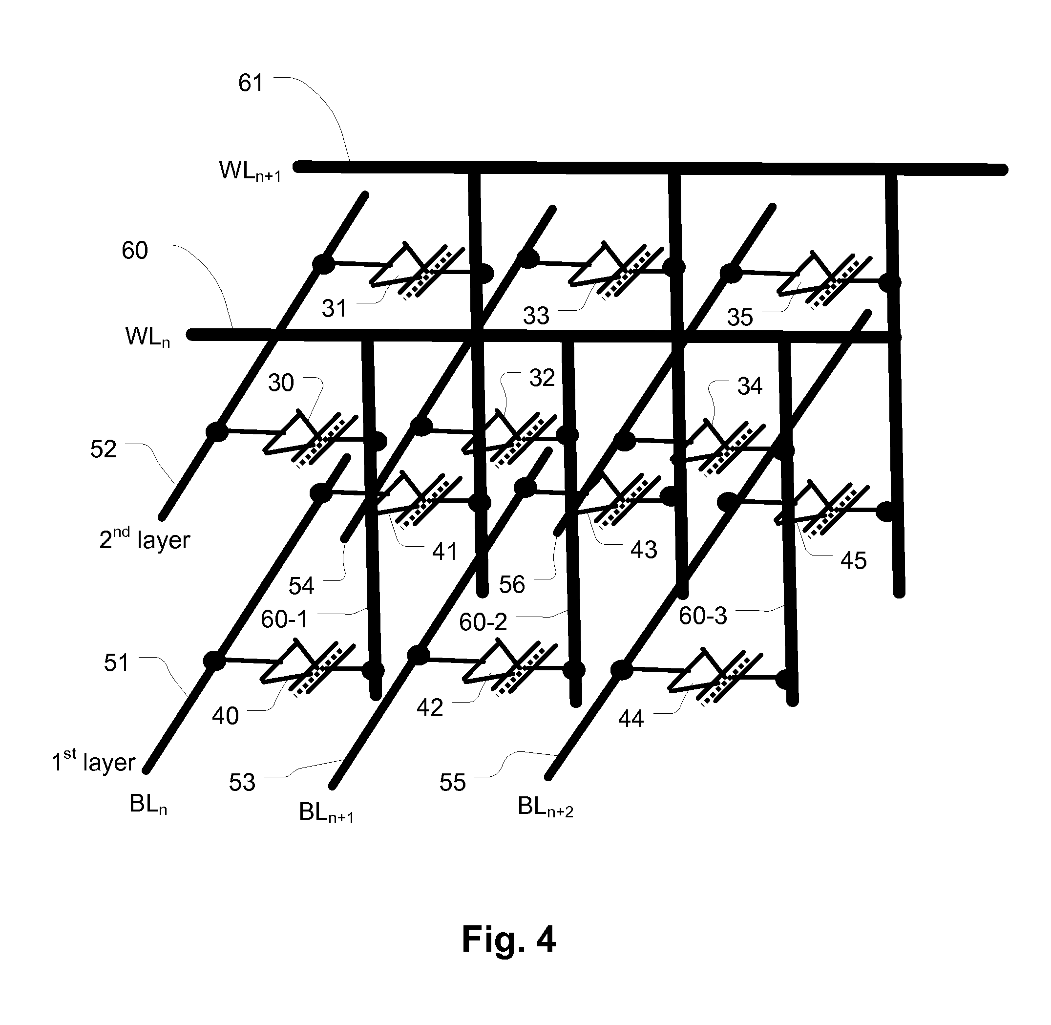
[0100]FIG. 1 is a perspective drawing of a 2×2 portion of a three-dimensional programmable resistance memory array with fill material removed from the drawing to give a view of the stacks of semiconductor material strips and orthogonal conductive lines that make up the 3D array. In this illustration, only 2 planes are shown. However, the number of planes can be extended to very large numbers. As shown in FIG. 1, the memory array is formed on an integrated circuit substrate having an insulating layer 10 over underlying semiconductor or other structures (not shown). The memory array includes a plurality of stacks of semiconductor material strips 11, 12, 13, 14 separated by insulating material 21, 22, 23, 24. The stacks are ridge-shaped extending on the Y-axis as illustrated in the figure, so that the semiconductor material strips 11-14 can be configured as strings. Semiconductor material strips 11 an...


PUM


Abstract

Various embodiments are directed to 3D memory arrays that lack a select line and devices controlled by the select line between one of the source line and the bit line, and the memory cells. Diodes between the other of source line and the bit line, and the memory cells provide needed isolation from the memory cells.

Description

REFERENCE TO RELATED APPLICATION[0001]This application claims the benefit of U.S. Provisional Patent Application No. 61 / 500,484 filed 23 Jun. 2011, which is incorporated herein by reference.BACKGROUND OF THE INVENTION[0002]1. Field of the Invention[0003]The present invention relates to high density memory devices, and particularly to memory devices in which multiple planes of memory cells are arranged to provide a three-dimensional 3D array.[0004]2. Description of Related Art[0005]As critical dimensions of devices in integrated circuits shrink to the limits of common memory cell technologies, designers have been looking to techniques for stacking multiple planes of memory cells to achieve greater storage capacity, and to achieve lower costs per bit. For example, thin film transistor techniques are applied to charge trapping memory technologies in Lai, et al., “A Multi-Layer Stackable Thin-Film Transistor (TFT) NAND-Type Flash Memory,” IEEE Int'l Electron Devices Meeting, 11-13 Dec. ...

Claims


Application Information

Patent Timeline
Patent Type & Authority Applications(United States)
IPC IPC(8): G11C16/04
CPCG11C5/02G11C13/0007G11C16/0483H01L27/11578H01L27/101H01L27/1021G11C2213/71H10B43/20H01L27/0688
Inventor LUE, HANG-TING
Owner MACRONIX INT CO LTD
Why Eureka
Try Eureka