Supercharge Your Innovation With Domain-Expert AI Agents!

Modular chip layout for active optical links

a module chip and active optical link technology, applied in the direction of lasers, electromagnetic transmission, transmission, etc., can solve the problem of increasing the waste of chip area

Active Publication Date: 2012-12-27
NVIDIA DENMARK APS
View PDF5 Cites 13 Cited by
  • Summary
  • Abstract
  • Description
  • Claims
  • Application Information

AI Technical Summary

Benefits of technology

[0008]The inventors has realized that the diversity of the present market for driver, transmitter and receiver chips (hereinafter “optical chips”) may be handled more efficiently. Today it is practice to design individual products of chips with the number of channels required for a specific application, e.g. a 4 channel driver chip is a different product / design from a 12 channel driver chip, even if the channel circuits are identical in function and / or layout.

Problems solved by technology

A lower number of channels per circuit increase the degree of freedom with which the number of channels on the chip can be selected, but may result in increased waste of chip area due to a high number of spacings relative to the number of channels.

Method used


Image

  • Modular chip layout for active optical links
  • Modular chip layout for active optical links
  • Modular chip layout for active optical links

Examples


Embodiment Construction

AND DETAILS OF THE INVENTION

[0039]The invention will be explained more fully below in connection with a preferred embodiment and with reference to the drawings:

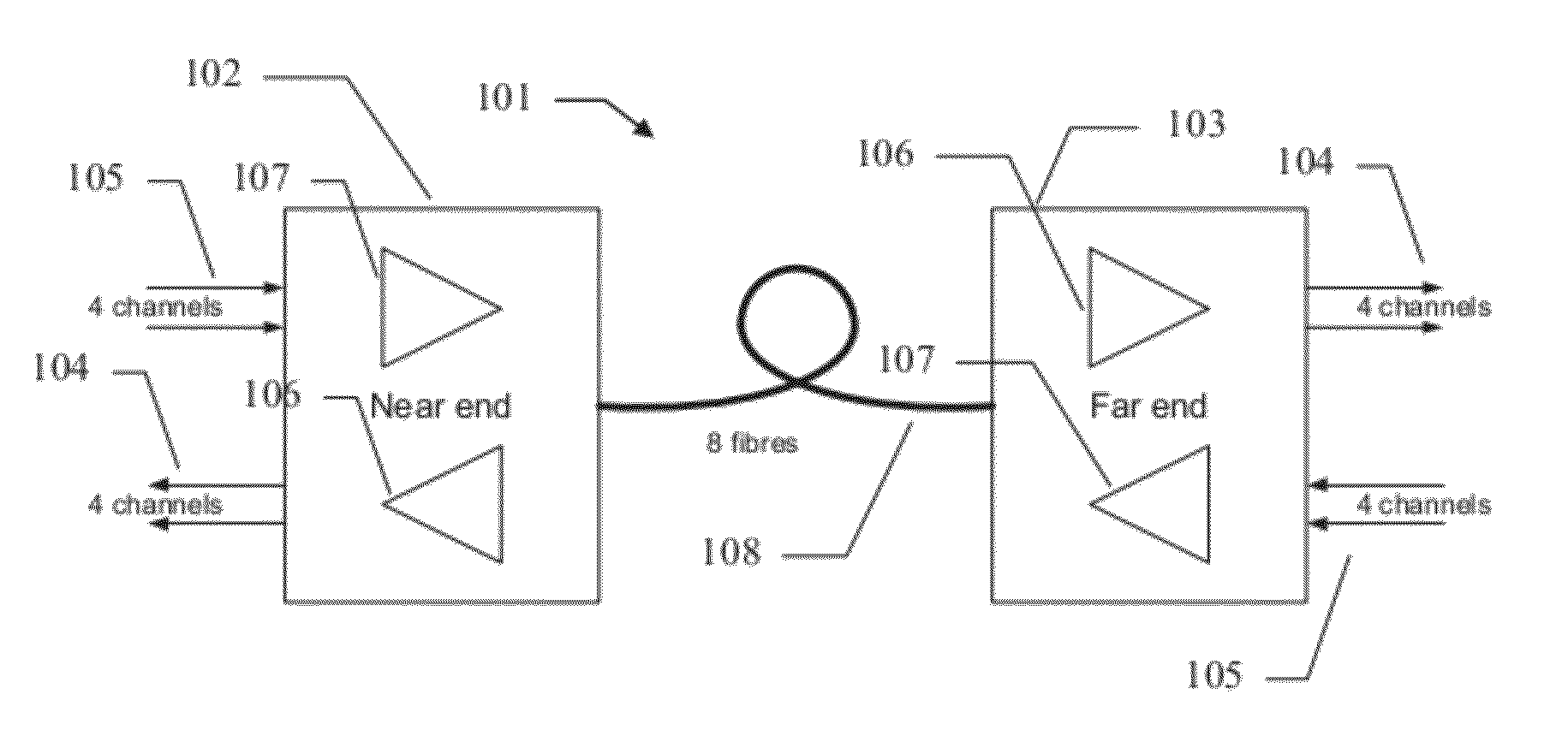
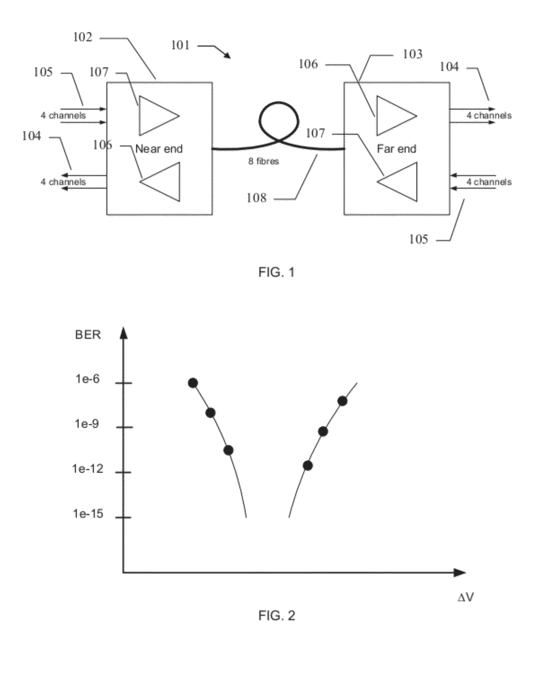
[0040]FIG. 1 shows an optical link with 4 channels in each direction

[0041]FIG. 2 shows Bath tub curve drawn based on measured error incidences (BER levels) as a function of decision threshold voltage.

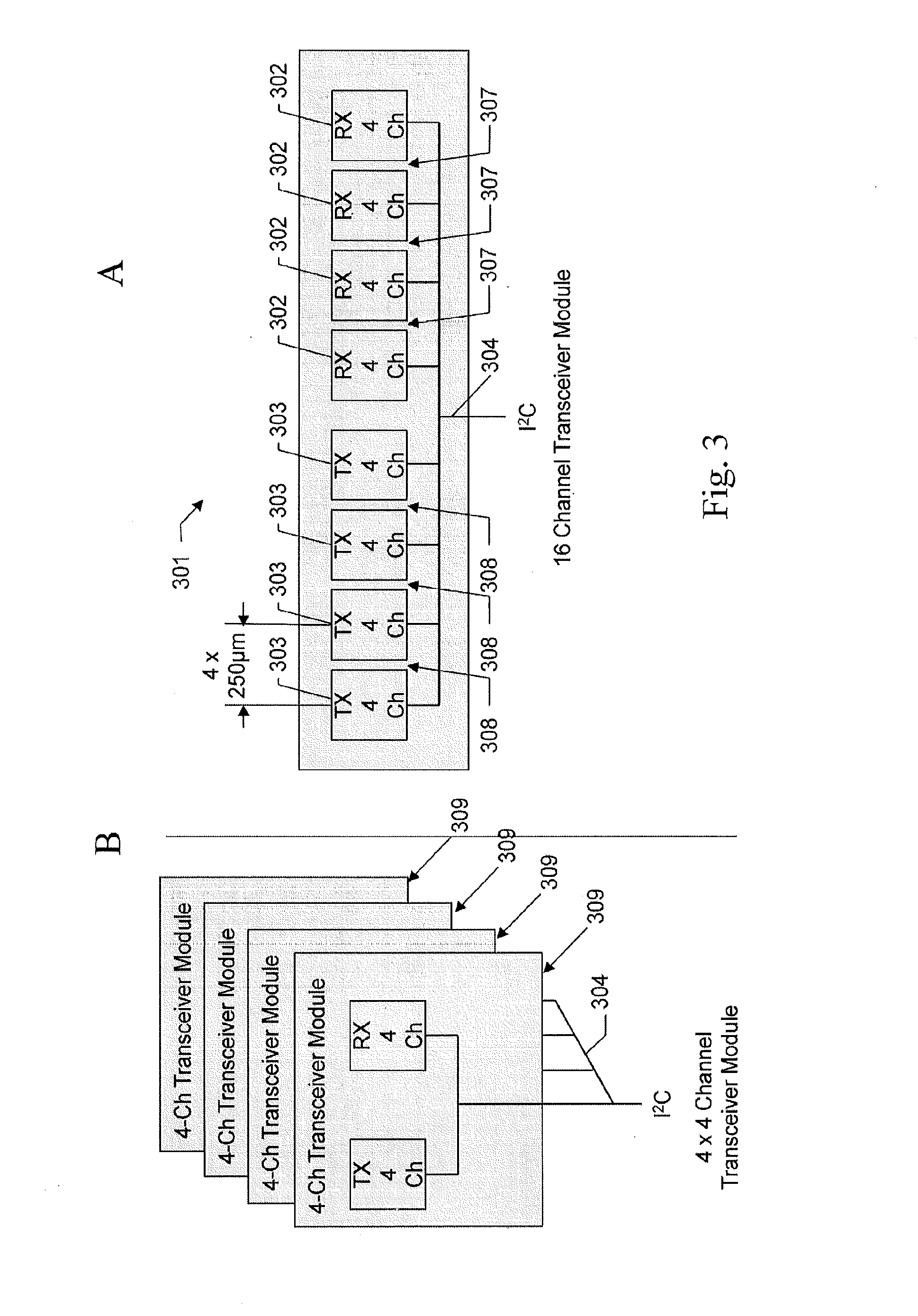
[0042]FIG. 3 shows 2 examples of modules with 16 channels using a shared I2C.

[0043]FIG. 4 shows a memory mapping and management application diagram example.

[0044]FIG. 5 shows an exemplary floor plan of a transmitter integrated circuit (here a VCSEL driver).

[0045]FIG. 6 shows an exemplary pad out and substrate board layout example with VIAs for mounting a single chip with two transmitter integrated circuits according to FIG. 5 in parallel—connected to a 1×8 VCSEL array on 250 μm pitch. VD 1 and VD 2 refers to VCSEL driver integrated circuit 1 and 2, respectively, each comprising 4 channels.

[0046]FIG. 7 show an exemplary floor plan...


PUM


Abstract

The present invention relates to a flexible method of provide chips for optical interconnect with different number of channels.

Description

[0001]In one embodiment this document describes the implementation of a chipset for a modular active optical link. In one embodiment the chipset consists of 4 Channel General Purpose transmitter and receiver.BACKGROUND[0002]One approach to support the communication requirements of the future includes utilizing optical interconnects, i.e. links, as an alternative to electrical wire-based interconnections. Currently, manufacturers produce products such as modules for optical interconnects and so-called optical cables. An optical module may be a transmitter (i.e. comprising a light source for transmitting an optical data signal), a receiver (i.e. comprising a photo detector for receiving an optical data signal) or a transceiver which is a combined receiver and transmitter. Often modules come with a connector for connecting one or more optical fibers for transporting the optical data signal. In an optical cable the module and fiber is typically pre-connected. It is also possible to have...

Claims


Application Information

Patent Timeline
Patent Type & Authority Applications(United States)
IPC IPC(8): G02B6/12H01L31/18
CPCH01S5/02276H01L2224/16225H04B10/801H01S5/423H01S5/02345
Inventor CHRISTENSEN, STEEN BAKFRANCK, THORKILD
Owner NVIDIA DENMARK APS
Features
  • R&D
  • Intellectual Property
  • Life Sciences
  • Materials
  • Tech Scout
  • Unparalleled Data Quality
  • Higher Quality Content
  • 60% Fewer Hallucinations
Learn More