Electric joint structure and method for preparing the same
- Summary
- Abstract
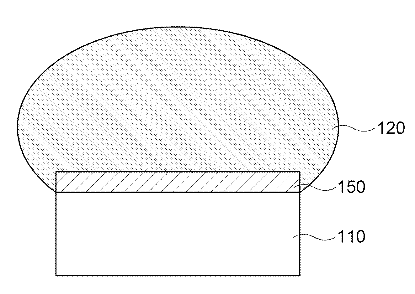
- Description
- Claims
- Application Information
AI Technical Summary
Benefits of technology
Problems solved by technology
Method used
Image

Examples
example
1) Electroless Ni Plating
[0072]The electroless nickel plating coating having a thickness of 0.1 μm was obtained by immersing the substrate subjected to the pre-treatment process in the electroless Ni plating solution (products available from TOP NICORON LPH-LF: OKUNO Co.) in a medium Ni—P type containing 6 to 9 wt % of phosphorus included in the plating coating at 75° C. for 1 minute and then, washing it for two minutes.
2) Electroless Pd Plating
[0073]The electroless palladium plating coating having a thickness of 0.1 μm was obtained by immersing the substrate to which the electroless Ni is plated in the electroless Pd plating solution, that is, XTP (P=3 wt %, products available from UYEMURA) at 50° C. for 10 minutes and washing it for two minutes.
3) Electroless Au Plating
[0074]The substrate to which the Pd is applied was immersed in the electroless gold plating solution, that is, GoBright TSB-72 (product available from UYEMURA Co.) at 80° C. for 5 minutes and washed for 2 minutes, a...
experimental example
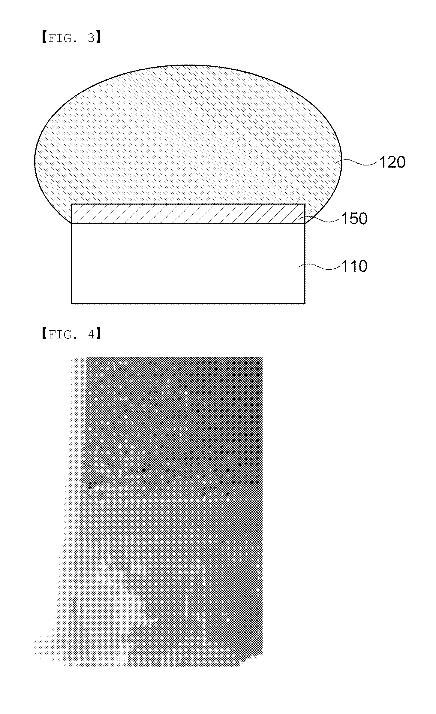
[0076]The cross section of the substrate subjected to the reflow process was observed by the scanning electron microscope and the observed results were shown in FIG. 4.
[0077]Next, it can be appreciated from FIG. 4 that the electric joint structure according to the exemplary embodiment of the present invention is provided with the copper joint, the intermetallic compound having the Cu—Sn—Pd—Ni, and the solder layer.
[0078]The structure of the intermetallic compound according to the exemplary embodiment of the present invention does not include the phosphorous component and does not include the Ni—Sn based intermetallic compound that may provide the cause of fracture of the related art. The results are effects obtained by minimizing the thickness of the nickel layer of the electroless surface treatment plating layer plated to the copper joint, which suppress the generation of the unwanted intermetallic compound to improve the impact resistance of the substrate and secure the reliabilit...
PUM
| Property | Measurement | Unit |
|---|---|---|
| Length | aaaaa | aaaaa |
| Thickness | aaaaa | aaaaa |
| Thickness | aaaaa | aaaaa |
Abstract
Description
Claims
Application Information
 - Generate Ideas
- Intellectual Property
- Life Sciences
- Materials
- Tech Scout
- Unparalleled Data Quality
- Higher Quality Content
- 60% Fewer Hallucinations
Browse by: Latest US Patents, China's latest patents, Technical Efficacy Thesaurus, Application Domain, Technology Topic, Popular Technical Reports.
© 2025 PatSnap. All rights reserved.Legal|Privacy policy|Modern Slavery Act Transparency Statement|Sitemap|About US| Contact US: help@patsnap.com