Semiconductor device comprising semiconductor substrate having diode region and IGBT region

Active Publication Date: 2013-01-03
DENSO CORP
View PDF1 Cites 37 Cited by
  • Summary
  • Abstract
  • Description
  • Claims
  • Application Information

AI Technical Summary

Benefits of technology

[0007]According to the configuration described above, the low impurity region whose electrical resistance is higher than both of the cathode region and the collector region is formed between the cathode region and the collector region. Since carriers are less likely to flow into the low impurity region with the high resistance, carrier density decreases in a region above

Problems solved by technology

As a result, the reverse recovery current of the diode increas

Method used


Image

  • Semiconductor device comprising semiconductor substrate having diode region and IGBT region
  • Semiconductor device comprising semiconductor substrate having diode region and IGBT region
  • Semiconductor device comprising semiconductor substrate having diode region and IGBT region

Examples


Example

First Example

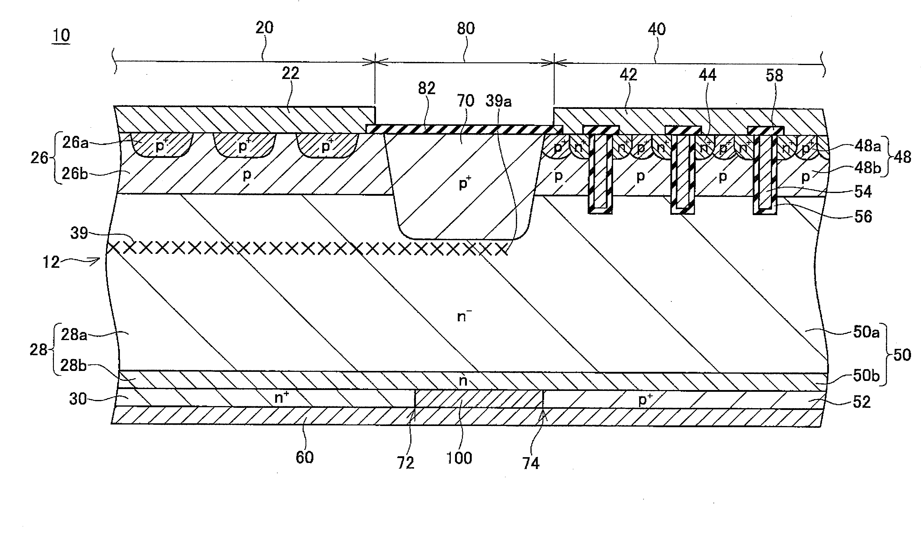
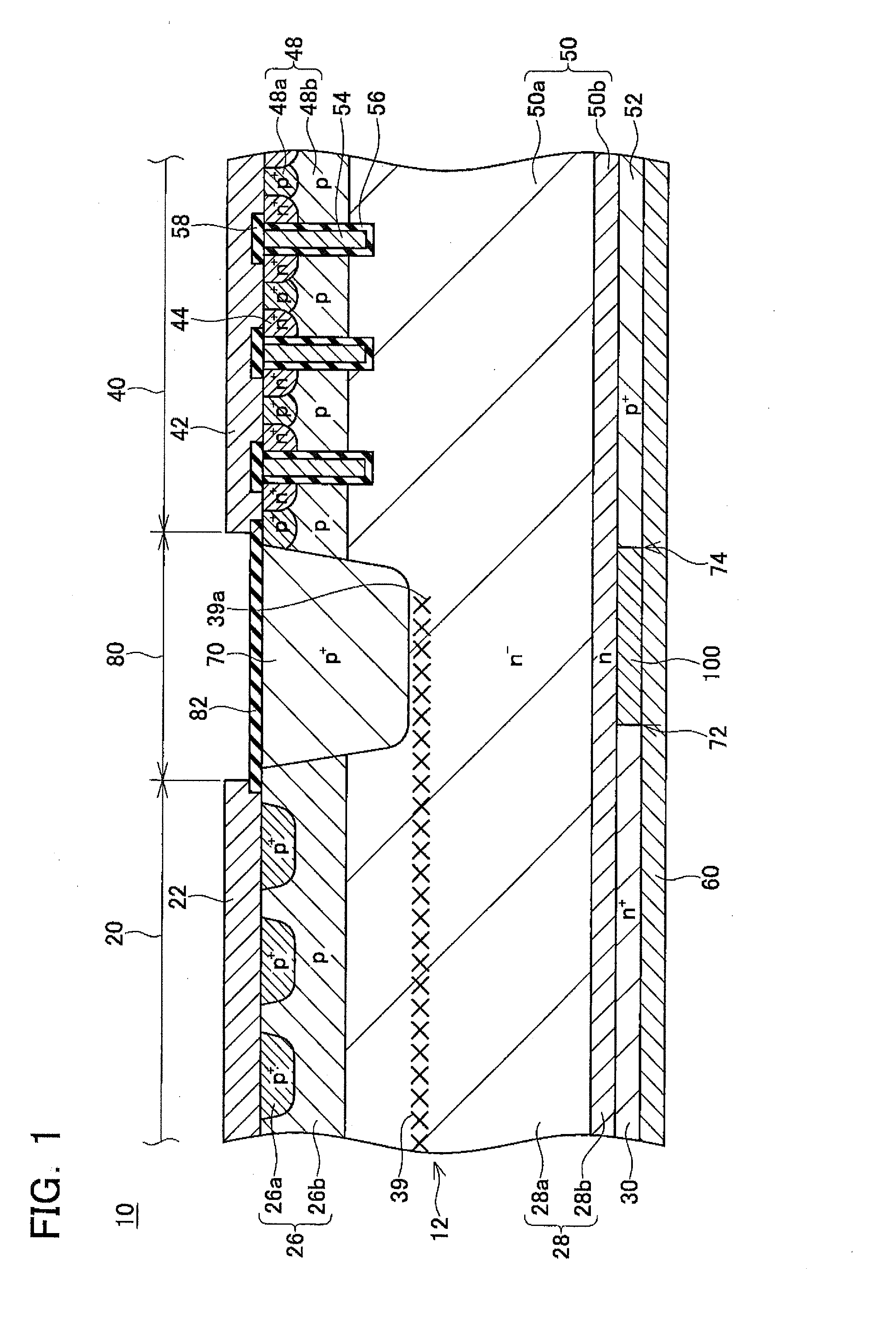
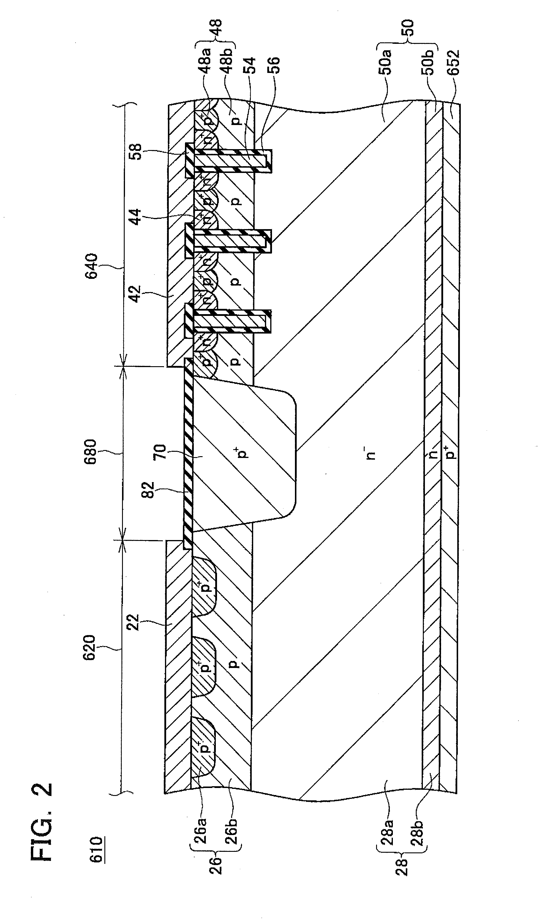
[0074]FIG. 2 is a diagram showing a cross section of a portion of the semiconductor wafer according to the first method for manufacturing the semiconductor device 10. A wafer 610 shown in FIG. 2 illustrates a state before the carrier lifetime control region 39, the cathode layer 30, the low impurity layer 100, and the common electrode 60 of the semiconductor device 10 are formed. Other components of the semiconductor device 10 have already been formed. A p-type collector layer 652 is formed on a lower surface side of the wafer 610. In the wafer 610, a diode forming region 620 denotes a region that becomes the diode region 20 of the semiconductor device 10 shown in FIG. 1 after a manufacturing step is completed, an IGBT forming region 640 denotes a region that becomes the IGBT region 40 of the semiconductor device 10 shown in FIG. 1 after the manufacturing step is completed, and a boundary forming region 680 denotes a region that becomes the boundary region 80 of the sem...

Example

Second Example

[0093]Since the masking step and the crystal defect forming step according to the second example are similar to those according to the first example of the first manufacturing method, a description thereof will be omitted. FIG. 12 shows a wafer 710 after steps up to the crystal defect forming step have been completed on the wafer 610 shown in FIG. 2. A carrier lifetime control region 39 is formed in an upper drift layer 28a of a diode drift layer 28 of the wafer 710. A mask 701 is disposed on a lower surface side of the wafer 710 in a same manner as in FIG. 4. In FIG. 12, components similar to those shown in FIGS. 1 and 2 are denoted by the same reference numerals.

[0094]Next, an ion doping step is performed. In the ion doping step, n-type impurity ions are doped to the lower surface of the wafer 710 and, as shown in FIG. 13, an ion doping region 730 doped with n-type ions is formed in a part of a collector layer 652 on the lower surface of the wafer 710.

[0095]Next, a l...

Example

Third Example

[0100]In the third example, after manufacturing a wafer 710 shown in FIG. 13 by a manufacturing step similar to that of the second example according to the second manufacturing method, a mask 701 is removed and annealing is performed. Consequently, a wafer 810 shown in FIG. 15 can be manufactured. In FIG. 15, components similar to those shown in FIGS. 1, 2, and 13 are denoted by the same reference numerals.

[0101]As shown in FIG. 15, an n-type cathode layer 830 and a p-type collector layer 852 are formed adjacent with each other on a lower surface side of the wafer 810. A boundary 121 is a boundary between the cathode layer 830 and the collector layer 852.

[0102]Laser annealing is performed on the boundary 121 on the lower surface side of the wafer 810 shown in FIG. 15. When laser annealing is performed by irradiating laser light on the boundary 121, the cathode layer 830 and the collector layer 852 in a vicinity of the boundary 121 are locally heated. As a result, n-type...


PUM


Abstract

A semiconductor device includes a semiconductor substrate in which a diode region and an IGBT region are formed, wherein a lower surface side of the semiconductor substrate comprises a low impurity region provided between a second conductivity type cathode region of the diode region and a first conductivity type collector region of the IGBT region. The low impurity region includes at least one of a first conductivity type first low impurity region which has a lower density of first conductivity type impurities than that in the collector region and a second conductivity type second low impurity region which has a lower density of second conductivity type impurities than that in the cathode region.

Description

CROSS-REFERENCE TO RELATED APPLICATION[0001]This application is a continuation of PCT application PCT / JP2010 / 056094 filed on Apr. 2, 2010 designating the United States of America, the entire contents of which are incorporated by reference herein.TECHNICAL FIELD[0002]The techniques described in the present specification relate to a semiconductor device comprising a semiconductor substrate in which a diode region and an IGBT region are formed.DESCRIPTION OF RELATED ART[0003]Japanese Patent Application Publication No. 2008-192737 discloses a semiconductor device comprising a semiconductor substrate in which a diode region and an IGBT region are formed. A lower surface side of the semiconductor substrate forms an n-type cathode layer in the diode region and a p-type collector layer in the IGBT region. The cathode layer and the collector layer are in contact with each other and a boundary therebetween exists within a boundary region between the diode region and the IGBT region.[0004]Carr...

Claims


Application Information

Patent Timeline
IPC IPC(8): H01L29/739H01L21/331
CPCH01L21/761H01L27/0761H01L29/861H01L29/32H01L29/7397H01L29/0834H01L27/04H01L21/76H01L21/265
Inventor IWASAKI, SHINYASOENO, AKITAKA
Owner DENSO CORP
Why Eureka
Try Eureka