

Copper wire receiving pad
a copper wire and receiving pad technology, applied in the field of electric connection, can solve problems such as the problem of increasing the criticality of the issu
- Summary
- Abstract
- Description
- Claims
- Application Information
AI Technical Summary
Benefits of technology
Problems solved by technology
Method used
Image

Examples
Embodiment Construction
[0035]For clarity, the same elements have been designated with the same reference numerals in the different drawings and, further, as usual in the representation of integrated circuits, the various drawings are not to scale.
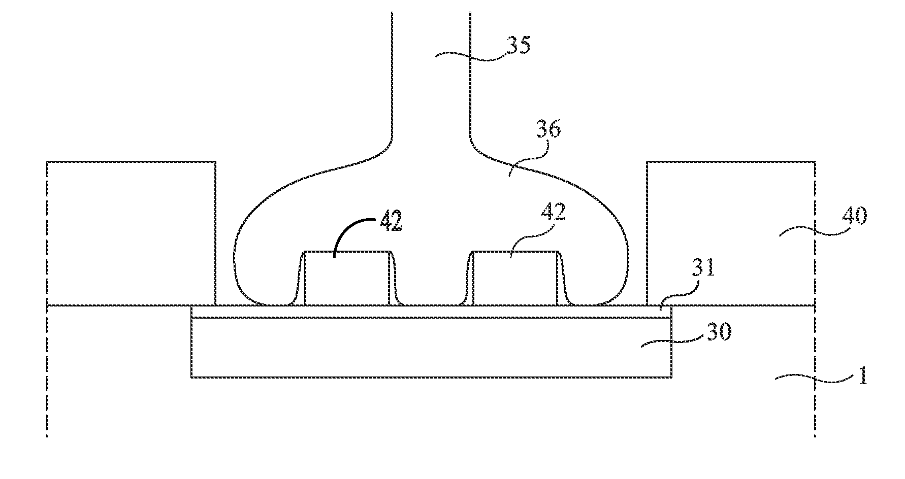
[0036]FIG. 3 shows a connection wire connected to a welding pad. The welding pad comprises on a copper pad 30 a barrier layer 31, for example, made of TiN, and an aluminum pad 32. The aluminum pad has a smaller surface area than the copper pad and the barrier layer topping this pad, whereby aluminum pad 32 is fully contained within the surface corresponding to the surface area of the copper pad. Once a copper wire 35 having a ball 36 formed at its end has been welded by ultrasounds on the pad surface, ball 36 is crushed. The dimension of the aluminum pad is such that after crushing, ball 36 comprises, on the one hand, a portion 38 in contact with the upper surface of aluminum pad 32, and on the other hand, a peripheral pad 39 which contacts barrier layer 31. In p...
PUM
| Property | Measurement | Unit |
|---|---|---|
| temperature | aaaaa | aaaaa |
| temperature | aaaaa | aaaaa |
| diameter | aaaaa | aaaaa |
Abstract
Description
Claims
Application Information