Driver circuit, method of manufacturing the driver circuit, and display device including the driver circuit

a driver circuit and display device technology, applied in pulse generators, pulse techniques, instruments, etc., can solve problems such as damage to transistors or electrodes, display devices being damaged by esd, and insufficient to prevent semiconductor elements, etc., to achieve the effect of suppressing the damage of semiconductor elements

Inactive Publication Date: 2013-01-03
SEMICON ENERGY LAB CO LTD
View PDF13 Cites 36 Cited by
  • Summary
  • Abstract
  • Description
  • Claims
  • Application Information

AI Technical Summary

Benefits of technology

[0010]In view of the above problem, one object of an embodiment of the disclosed invention is to provide a driver circuit which suppresses damage of a semiconductor element due to ESD in a manufacturing process, and a method of manufacturing the driver circuit. Another object of an embodiment of the disclosed invention is to provide a driver circuit provided with a protection circuit with low leakage current, and a method of manufacturing the driver circuit.
[0011]According to the disclosed invention, a protection circuit is provided in a driver circuit to be electrically connected to a semiconductor element in the driver circuit. A transistor which serves as the semiconductor element in the driver circuit and a transistor included in the protection circuit in the driver circuit are formed at the same time; as a result, it is possible to suppress damage of the semiconductor element due to ESD in the manufacturing process of the driver circuit. Further, according to the disclosed invention, the transistor included in the protection circuit in the driver circuit includes an oxide semiconductor film, so that leakage current in the protection circuit can be reduced.
[0027]According to an embodiment of the disclosed invention, it is possible to provide a driver circuit which suppresses damage of a semiconductor element due to ESD in a manufacturing process, and a method of manufacturing the driver circuit. According to an embodiment of the disclosed invention, it is also possible to provide a driver circuit provided with a protection circuit with low leakage current, and a method of manufacturing the driver circuit.

Problems solved by technology

However, only the protection circuit formed between the scan electrode of the display device and the conductive line provided in the periphery of the display portion, as described in Patent Document 1, is not sufficient to prevent a semiconductor element such as a transistor provided in a driver circuit of the display device from being damaged by ESD.
In particular, when a plasma treatment is performed in a process of manufacturing a transistor in the driver circuit, plasma damage causes ESD in manufacture of the transistor, which may result in damage of the transistor or an electrode.
Therefore, in the case where a protection circuit including such an element is connected between a power supply line and a wiring such as a signal line provided in a driver circuit, leakage current may flow between the wirings to change the potentials of the wirings or the power supply potential, causing unstable operation of the driver circuit.

Method used


Image

  • Driver circuit, method of manufacturing the driver circuit, and display device including the driver circuit
  • Driver circuit, method of manufacturing the driver circuit, and display device including the driver circuit
  • Driver circuit, method of manufacturing the driver circuit, and display device including the driver circuit

Examples


embodiment 1

[0048]In this embodiment, configurations and operation methods of a driver circuit and a protection circuit which can be used in the driver circuit, according to an embodiment of the disclosed invention, will be described with reference to FIG. 1, FIG. 2, FIGS. 3A and 3B, and FIGS. 4A and 4B.

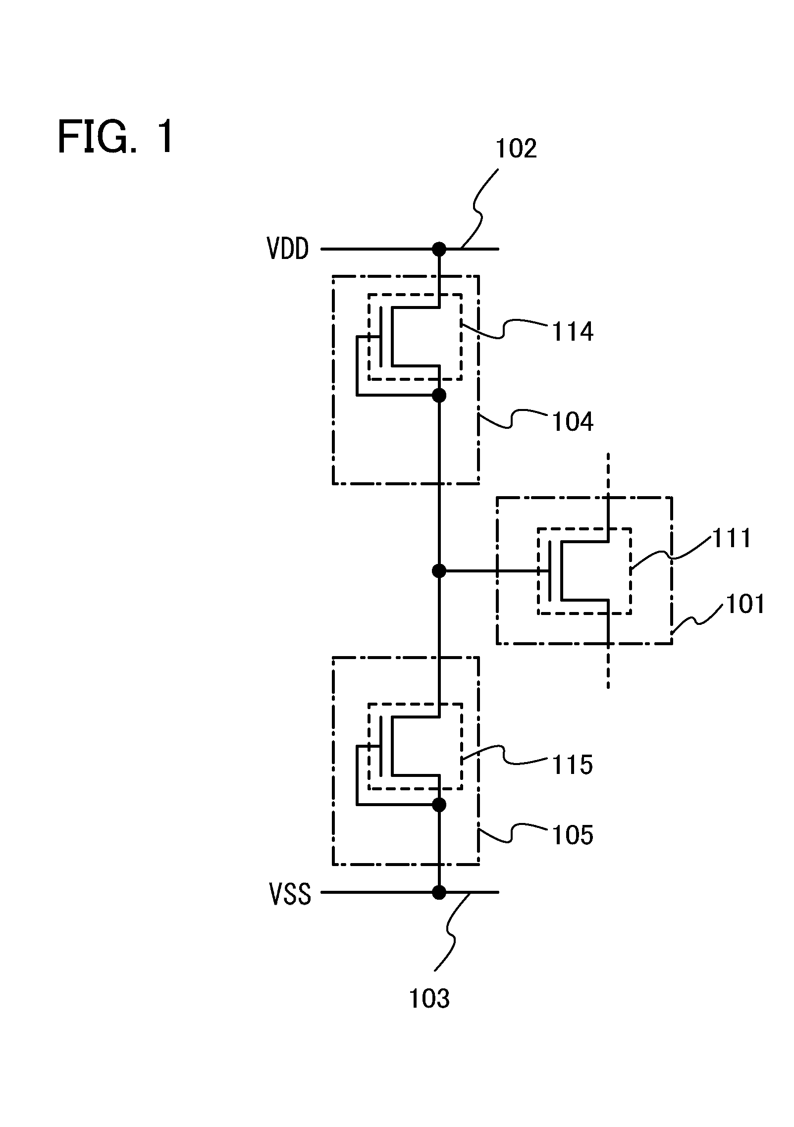
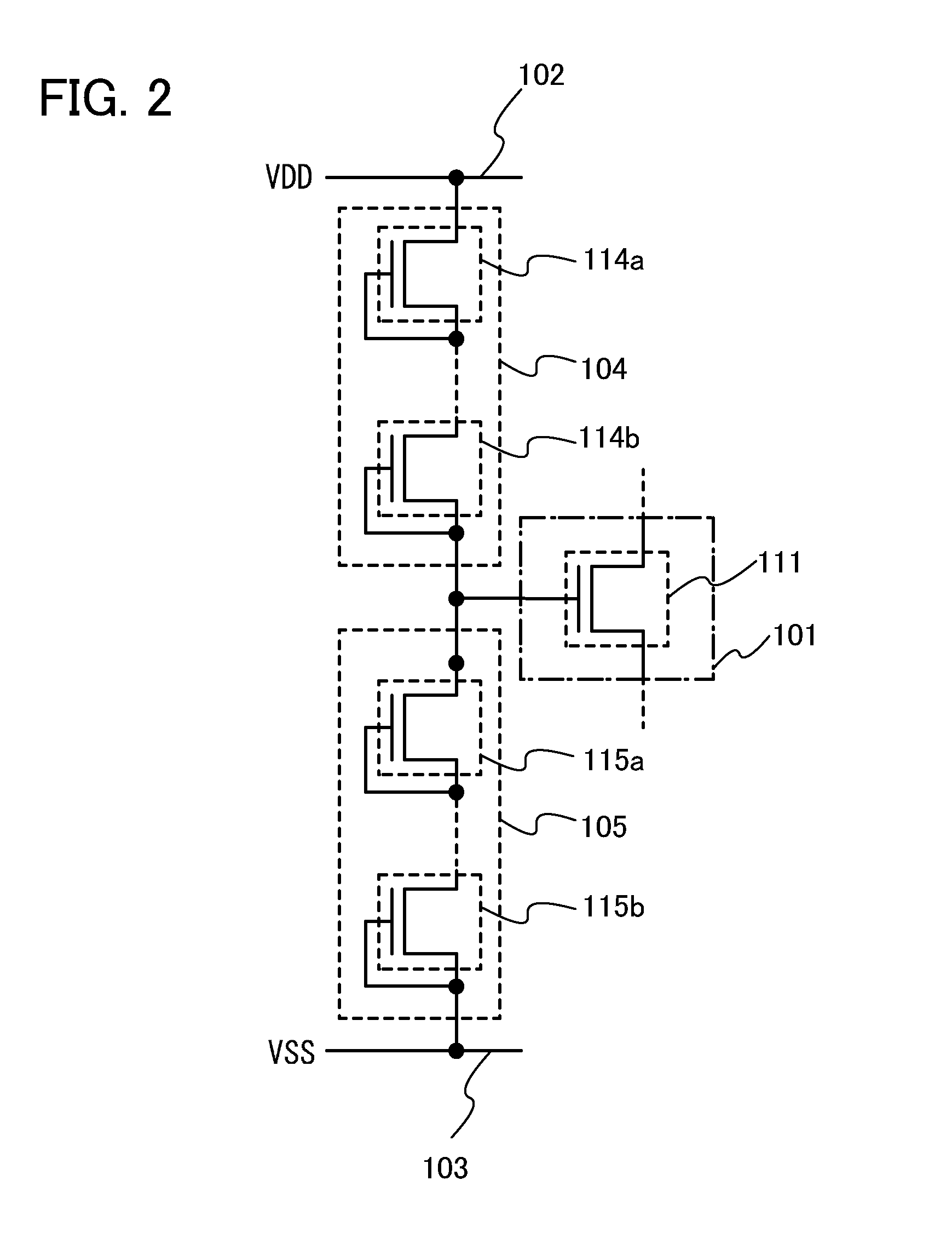
[0049]FIG. 1 illustrates a connection relation between protection circuits used in a driver circuit and a semiconductor element included in the driver circuit, according to an embodiment of the disclosed invention. In the driver circuit, a first protection circuit 104 is provided between one of terminals of a semiconductor element 101 included in the driver circuit and a first wiring 102, and a second protection circuit 105 is provided between the one of the terminals of the semiconductor element 101 included in the driver circuit and a second wiring 103. In the driver circuit in FIG. 1, the first wiring 102 can be a high-potential power supply line (VDD) and the second wiring 103 can be a low-p...

embodiment 2

[0110]In this embodiment, a method of manufacturing the driver circuit described in Embodiment 1 will be described with reference to FIGS. 8A to 8F and FIGS. 9A to 9D. As an example, a method of manufacturing a transistor 440 and a transistor 450 at the same time, which is illustrated in FIGS. 8A to 8F, is described. Here, the transistor 440 corresponds to the transistor 114 included in the first protection circuit 104 in Embodiment 1 and the transistor 450 corresponds to the transistor 111 serving as the semiconductor element 101 in Embodiment 1. Although not shown directly in this embodiment, the transistor 115 included in the second protection circuit 105 in Embodiment 1 can be formed in a manner similar to that for the transistor 440. In the case where a driver circuit portion and a display portion are manufactured over the same substrate as illustrated in FIGS. 3A and 3B, a transistor in the display portion can also be formed in a similar manner.

[0111]As illustrated in FIG. 8F,...

embodiment 3

[0238]In this embodiment, a method of manufacturing a driver circuit including transistors the structures of which are different from those of the transistors in Embodiment 2 will be described with reference to FIGS. 10A to 10C. As an example, a method of forming a transistor 460 and a transistor 470 at the same time in FIGS. 10A to 10C is described. Here, the transistor 460 corresponds to the transistor 440 in Embodiment 2, i.e., the transistor 114 included in the first protection circuit 104, whereas the transistor 470 corresponds to the transistor 450 in Embodiment 2, i.e., the transistor 111 serving as the semiconductor element 101. Although not shown directly in this embodiment either, the transistor 115 included in the second protection circuit 105 in the above embodiments can be manufactured in a manner similar to that for the transistor 460. In the case where a display portion is provided over the same substrate as the driver circuit portion as in FIGS. 3A and 3B, transistor...


PUM

PropertyMeasurementUnit
band gapaaaaaaaaaa
band gapaaaaaaaaaa
band gapaaaaaaaaaa

Abstract

Provided are a driver circuit which suppresses damage of a semiconductor element due to ESD in a manufacturing process, a method of manufacturing the driver circuit. Further provided are a driver circuit provided with a protection circuit with low leakage current, and a method of manufacturing the driver circuit. By providing a protection circuit in a driver circuit to be electrically connected to a semiconductor element in the driver circuit, and by forming, at the same time, a transistor which serves as the semiconductor element in the driver circuit and a transistor included in the protection circuit in the driver circuit, damage of the semiconductor element due to ESD is suppressed in the process of manufacturing the driver circuit. Further, by using an oxide semiconductor film for the transistor included in the protection circuit in the driver circuit, leakage current in the protection circuit is reduced.

Description

BACKGROUND OF THE INVENTION[0001]1. Field of the Invention[0002]The present invention relates to a driver circuit provided with a protection circuit for preventing damage of the circuit in a case where a high voltage such as electrostatic discharge is applied. The invention also relates to a method of manufacturing the driver circuit and a display device including the driver circuit.[0003]2. Description of the Related Art[0004]In a semiconductor circuit used in a semiconductor device such as a display device, a semiconductor element, an electrode, or the like could be damaged by electrostatic discharge (hereinafter referred to as “ESD”). As a measure to prevent damage of a semiconductor circuit due to ESD, a protection circuit is connected to a semiconductor circuit in many cases. A protection circuit refers to a circuit for preventing overvoltage applied to a terminal, a wiring, or the like from being supplied to a semiconductor circuit. A resistor, a diode, a transistor, and a cap...

Claims


Application Information

Patent Timeline
Patent Type & Authority Applications(United States)
IPC IPC(8): H03K17/00H01R43/00
CPCG11C19/28G09G2310/0267G09G2310/0275G09G2310/0286G09G2330/04Y10T428/2438G09G3/3688H02H9/044Y10T428/24364Y10T29/49117Y10T428/24372G09G3/3283H01L27/0248H01L29/66742H01L29/7869H01L27/0266H01L27/1225G09G3/3677G09G2300/0426
Inventor YAMAZAKI, SHUNPEIKOYAMA, JUN
Owner SEMICON ENERGY LAB CO LTD
Why Eureka
Try Eureka