Power factor correction converter and power factor correction conversion device

a conversion device and power factor technology, applied in the direction of conversion with intermediate conversion to dc, efficient power electronics conversion, energy industry, etc., can solve the problems of large size, low conversion efficiency and power density, and great effect of current passing through a switching transistor. achieve the effect of improving conversion efficiency, small circuit size and improving power density

Active Publication Date: 2013-01-03
HUAWEI DIGITAL POWER TECH CO LTD
View PDF5 Cites 24 Cited by
  • Summary
  • Abstract
  • Description
  • Claims
  • Application Information

AI Technical Summary

Benefits of technology

[0009]By taking two groups of bidirectional switches as an example, in the power factor correction converter provided in an embodiment of the present invention, a boost inductor, an autotransformer, and two groups of bidirectional switches form a tristate switch unit circuit, which includes three working states: two groups of bidirectional switches being turned on simultaneously, two groups of bidirectional switches being turned off simultaneously, and one group of bidirectional switches being turned on and the other group of bidirectional switches being turned off. To achieve better technical effect, an autotransformer in which two coils have the same number of turns can be selected.
[0010]Compared with the prior art, the foregoing technical solutions provided in the present invention have the following advantages. When a tristate switch unit circuit is used, the boost inductor is charged twice and discharged twice in one switching period, ripples on the boost inductor and the bus filter capacitor are reduced and the effective value of the current passing through a transistor of a bidirectional switch becomes smaller, thereby improving the conversion efficiency. In addition, the frequency of the ripple on the boost inductor is twice as much as that of a switch, so that the inductance of the boost inductor is decreased by 50%, which makes the size of the circuit smaller and the power density higher, thereby solving the technical problems of the low conversion efficiency and power density in the prior art.
[0011]When three or more groups of bidirectional switches are used, a multistate switch unit circuit formed by a boost inductor, an autotransformer, and multiple groups of bidirectional switches has four or more working states. Each case includes two states, that is, each group of bidirectional switches being turned on simultaneously and each group of bidirectional switches being turned off simultaneously, and more working states that occur when some bidirectional switches are turned on and some bidirectional switches are turned off. In one switching period, the number of times that a boost inductor is charged and discharged is equal to the number of groups of bidirectional switches. Therefore, when more groups of bidirectional switches are used, the ripple on the boost inductor becomes smaller, so that the inductance of the boost inductor is further decreased, thereby improving the conversion efficiency and power density.

Problems solved by technology

However, in the interleaving technology, the peak voltages at two ends of a boost inductor are 400 V, the inductance ripple current is high, the effective value of the current passing through a switching transistor is great, and the size is large.
Therefore, the conversion efficiency and the power density are low.

Method used


Image

  • Power factor correction converter and power factor correction conversion device
  • Power factor correction converter and power factor correction conversion device
  • Power factor correction converter and power factor correction conversion device

Examples


embodiment 1

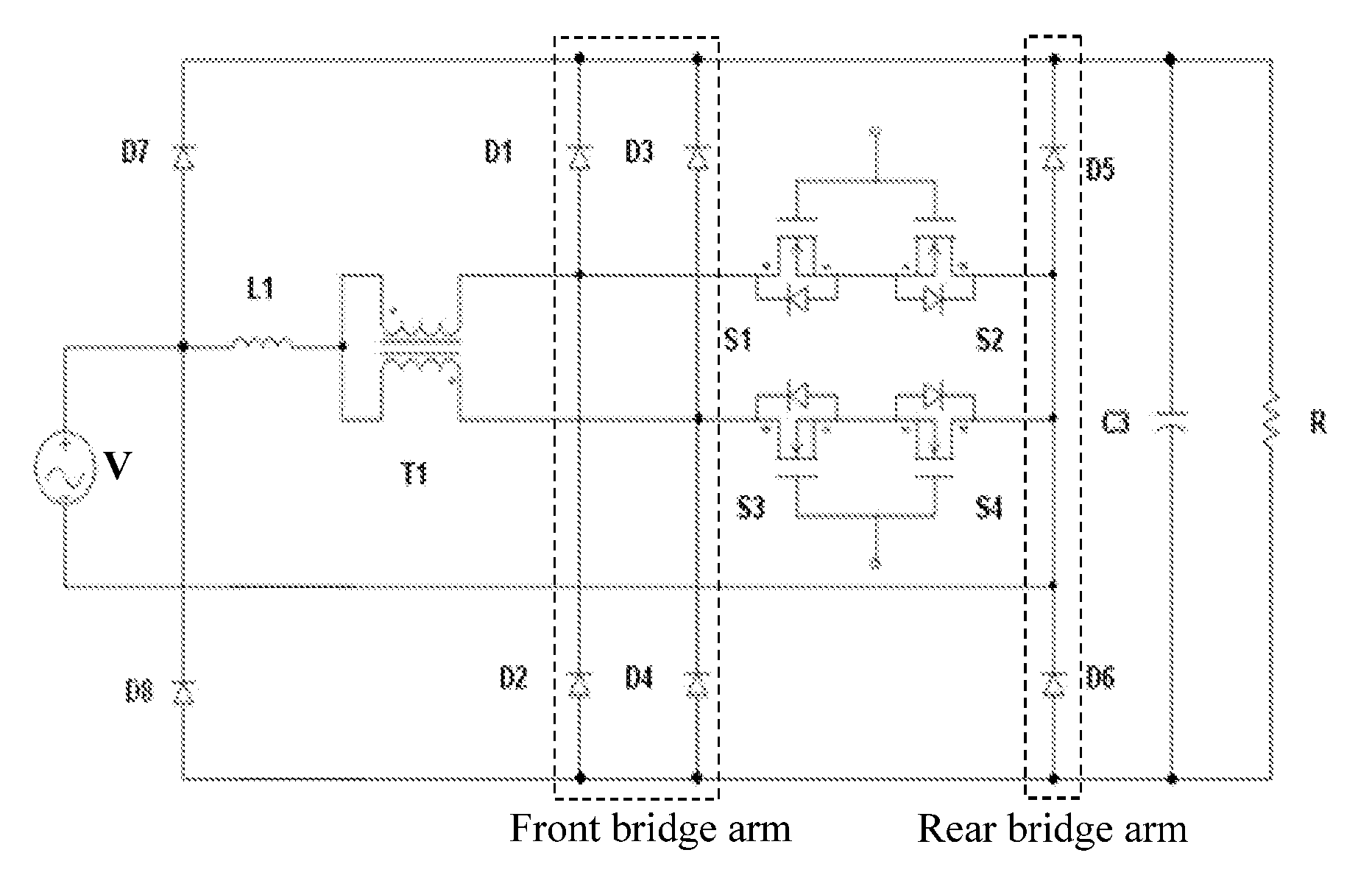
[0027]As shown in FIG. 1, a power factor correction converter provided in an embodiment of the present invention includes two groups of bidirectional switches, that is, S1-S2 and S3-S4. Since coils in an autotransformer T1, front bridge arms, and the groups of the bidirectional switch are in one-to-one correspondence, both the number of the coils in the autotransformer and the number of the front bridge arms both are 2 according to the embodiment of the present invention. Furthermore, to achieve better technical effect, the autotransformer T1 in which two coils have the same number of turns is selected.

[0028]As an exemplary solution, the power factor correction converter according to the embodiment of the present invention further includes a protective bridge arm, the protective bridge arm includes two protective diodes D7 and D8 unidirectionally connected in series, an intermediate connection point located between D7 and D8 is connected to an input end of a boost inductor L1, and t...

embodiment 2

[0050]This embodiment is similar to Embodiment 1. The difference is that, as shown in FIG. 10, in this embodiment, a boost inductor is integrated in an autotransformer. For an application requiring low power, a boost inductor can be integrated in the autotransformer, so that a required boost induction value is obtained by adjusting a coupling coefficient M of the autotransformer, to further decrease the size and cost of a converter.

embodiment 3

[0051]This embodiment is similar to Embodiment 1. The difference is that, as shown in FIG. 11, in this embodiment, two clamped capacitors C1 and C2, which are configured to suppress common mode noise interference, are further included, where one end of the clamped capacitor C1 and one end of the clamped capacitor C2 are correspondingly connected to two ends of the AC input power grid, and the other end of the clamped capacitor C1 and the other end of the clamped capacitor C2 connected to each other are connected to one end of the bus filter capacitor C3. The two clamped capacitors C1 and C2 are capable of suppressing electromagnetic interference, especially common mode noise interference.

[0052]An embodiment of the present invention also provides a power factor correction conversion device. The power factor correction conversion device includes the foregoing power factor correction converter, an AC input power grid, and a load, where one end of the AC input power grid is connected to...


PUM


Abstract

A power factor correction converter and a power factor correction conversion device, includes two groups of bidirectional switches, an autotransformer, a boost inductor, a bus filter capacitor, two front bridge arms; and a rear bridge arm; the front end of each group of bidirectional switches are connected to a coil of the autotransformer in one-to-one correspondence, and a rear end of each group of bidirectional switches is connected to one end of an AC input power grid; a central tap of the autotransformer is connected to an output end of the boost inductor, and an input end of the boost inductor is connected to the other end of the AC input power grid; a front end of each group of bidirectional switches is connected to a front bridge arm, and a rear end is connected to the rear bridge arm.

Description

CROSS-REFERENCE TO RELATED APPLICATIONS[0001]This application is a continuation of International Application No. PCT / CN2011 / 076781, filed on Jul. 1, 2011, which is hereby incorporated by reference in its entirety.FIELD OF THE INVENTION[0002]The present invention relates to the field of power rectification technologies, and in particular, to a power factor correction converter and a power factor correction conversion device.BACKGROUND OF THE INVENTION[0003]A rectifier module of the communications power supply usually consists of a two-stage circuit topology, where the main function of a pre-stage power factor correction (Power Factor Correction, PFC) circuit is to implement the power factor correction, and at the same time provide a post-stage direct current-direct current (DC-DC) conversion circuit with a stable high-voltage DC input (usually 400 V) which is not isolated from the power grid. The post-stage DC-DC conversion circuit then converts the non-isolated DC high voltage into ...

Claims


Application Information

Patent Timeline
Patent Type & Authority Applications(United States)
IPC IPC(8): H02M1/12
CPCY02B70/126H02M7/219H02M2001/0064H02M1/4225H02M3/1584H02M1/4208Y02B70/10Y02P80/10H02M1/0064H02M1/0085
Inventor PAN, DENGHAI
Owner HUAWEI DIGITAL POWER TECH CO LTD
Why Eureka
Try Eureka