Method for manufacturing polycrystalline silicon ingot, and polycrystalline silicon ingot

Active Publication Date: 2013-01-10
MITSUBISHI MATERIALS ELECTRONICS CHEM CO LTD
View PDF2 Cites 4 Cited by
  • Summary
  • Abstract
  • Description
  • Claims
  • Application Information

AI Technical Summary

Benefits of technology

[0048]Thus, according to the present invention, the method for manufacturing a polycrystalline silicon ingot, which is allowed to cast the polycrystalline silicon ingot by decreasing in portion ha

Problems solved by technology

In particular, higher amount of oxygen and impurities in the polycrystalline silico

Method used


Image

  • Method for manufacturing polycrystalline silicon ingot, and polycrystalline silicon ingot
  • Method for manufacturing polycrystalline silicon ingot, and polycrystalline silicon ingot
  • Method for manufacturing polycrystalline silicon ingot, and polycrystalline silicon ingot

Examples


examples

[0100]The results of the confirmatory experiment conducted to confirm advantageous effects of the present invention are reported below. The polycrystalline silicon ingot in size of 680 mm squares x 300 mm in height was cast by using the polycrystalline silicon ingot manufacturing apparatus described in the present embodiment.

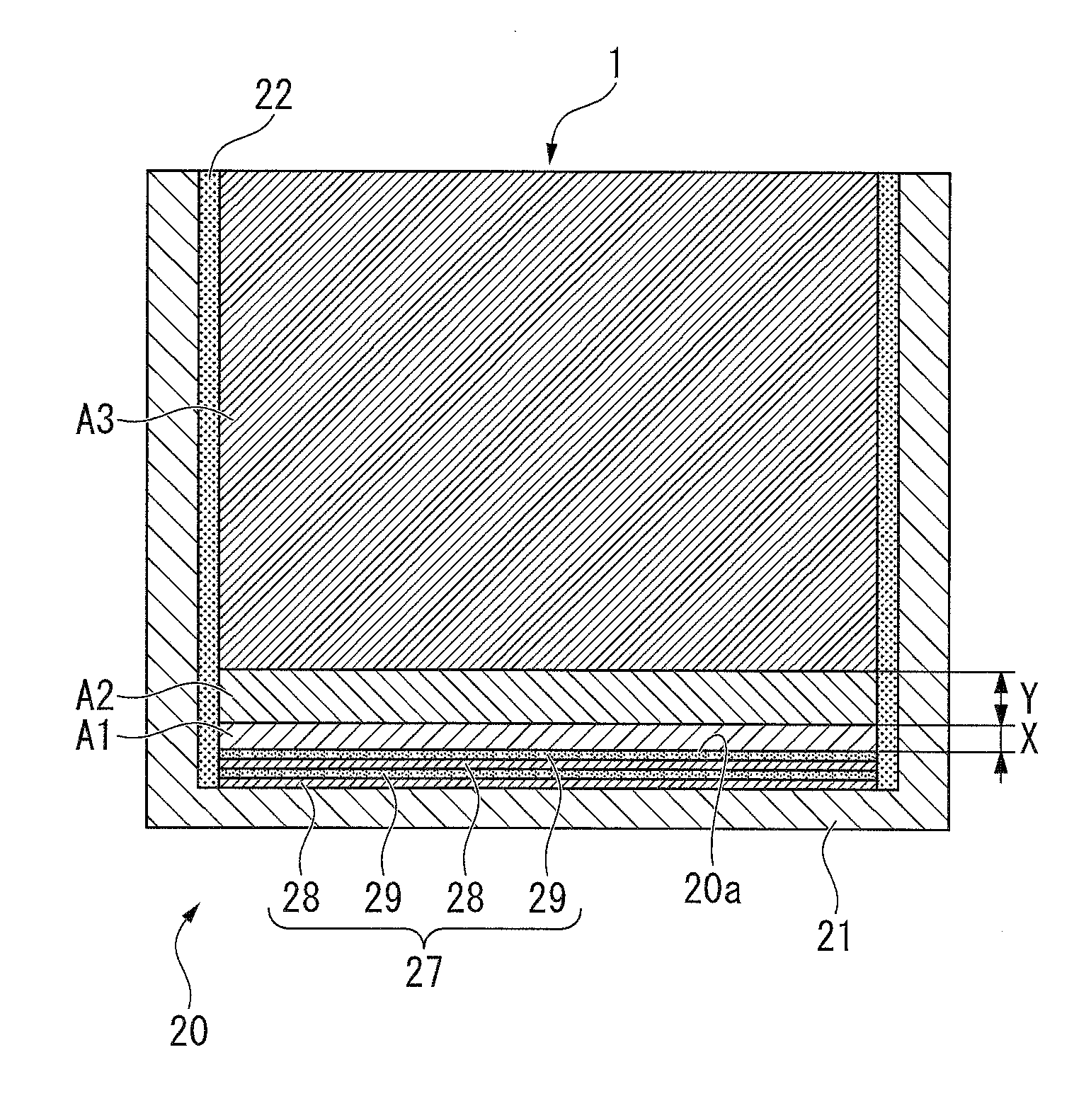
[0101]In Inventive Example, as shown in FIG. 4, the polycrystalline silicon ingot was cast using a crucible having a Si3N4 coating layer formed on its inner face and a multilayered silica coating layer formed on the inside of its bottom, with modification of the solidification rate in the patterns described in the above-mentioned embodiment. Namely, as shown in FIG. 6, the solidification rate V1 in the first zone Al from the bottom to 20 mm in height was set to 15 mm / h, the solidification rate V2 in the second zone A2 from 20 mm to 40 mm in height was set to 3 mm / h and the solidification rate V3 in the third zone A3 from 40 mm to 300 mm in height was set to 5.8 ...


PUM

PropertyMeasurementUnit
Lengthaaaaaaaaaa
Lengthaaaaaaaaaa
Lengthaaaaaaaaaa

Abstract

A method for manufacturing a polycrystalline silicon ingot includes unidirectionally solidifying a molten silicon upwardly from the bottom of a crucible, wherein the crucible is provided with silica deposited on the bottom of the crusible; and then dividing the degree of solidification in the crucible into a first zone from 0 mm to X in height (10 mm≦X<30 mm), a second zone from X to Y in height (30 min≦Y<100 mm) and a third zone of Y or more in height, based on the bottom of the crucible, wherein a solidification rate V1 in the first zone is set in the range of 10 mm/h≦V1≦20 mm/h and a solidification rate V2 in the second zone is set in the range of 1 mm/h≦V2≦5 mm/h.

Description

CROSS-REFERENCE TO RELATED PATENT APPLICATIONS[0001]This application is a U.S. National Phase Application under 35 U.S.C. §371 of International Patent Application No. PCT / JP2011 / 057361, filed Mar. 25, 2011, and claims the benefit of Japanese Patent Application No. 2010-071700, filed Mar. 26, 2010, all of which are incorporated by reference herein. The International Application was published in Japanese on Sep. 29, 2011 as International Publication No. WO / 2011 / 118773 under PCT Article 21(2).FIELD OF THE INVENTION[0002]The present invention is related to a method for manufacturing a polycrystalline silicon ingot by unidirectionally solidifying a silicon melt in a silica crucible to cast the polycrystalline silicon ingot, and the polycrystalline silicon ingot obtained by the method.BACKGROUND OF THE INVENTION[0003]A polycrystalline silicon ingot has been used as a material for a solar cell substrate, for example, as disclosed in Patent Document 1. Namely, the polycrystalline silicon in...

Claims


Application Information

Patent Timeline
IPC IPC(8): C30B11/00
CPCC01B33/021C30B11/00C30B29/06C30B11/003C30B11/002B22D27/04C01B33/02
Inventor TSUZUKIHASHI, KOJIIKEDA, HIROSHIKANAI, MASAHIROWAKITA, SABURO
Owner MITSUBISHI MATERIALS ELECTRONICS CHEM CO LTD
Why Eureka
Try Eureka