Method and apparatus for remote plasma source assisted silicon-containing film deposition

a technology of plasma source and film deposition method, which is applied in the direction of sustainable manufacturing/processing, final product manufacturing, coatings, etc., can solve the problems of particle generation, inefficient film deposition, physical and electrically inferior and unstable deposited films,

Inactive Publication Date: 2013-01-10
APPLIED MATERIALS INC
View PDF0 Cites 106 Cited by
  • Summary
  • Abstract
  • Description
  • Claims
  • Application Information

AI Technical Summary

Problems solved by technology

However, problems exist in current production equipment and methods used in the deposition of these films.
For example, in conventional thermal chemical vapor deposition and plasma enhanced chemical vapor deposition (PECVD) processes, the low energy ...

Method used


Image

  • Method and apparatus for remote plasma source assisted silicon-containing film deposition
  • Method and apparatus for remote plasma source assisted silicon-containing film deposition
  • Method and apparatus for remote plasma source assisted silicon-containing film deposition

Examples


Embodiment Construction

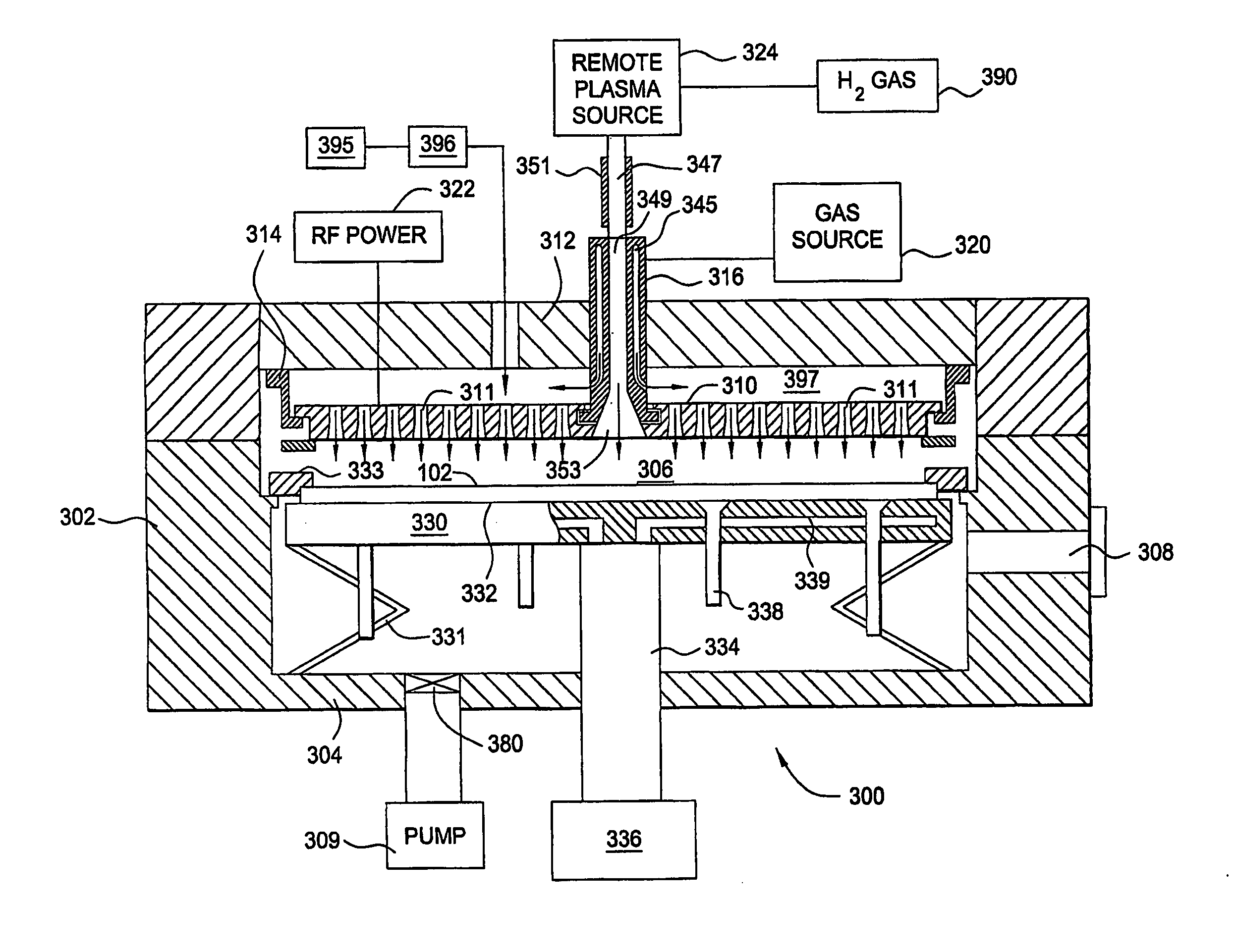
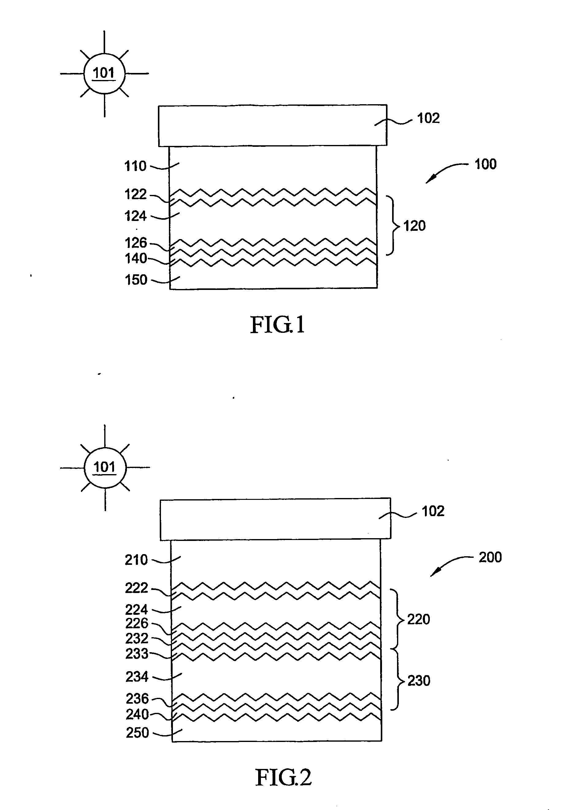
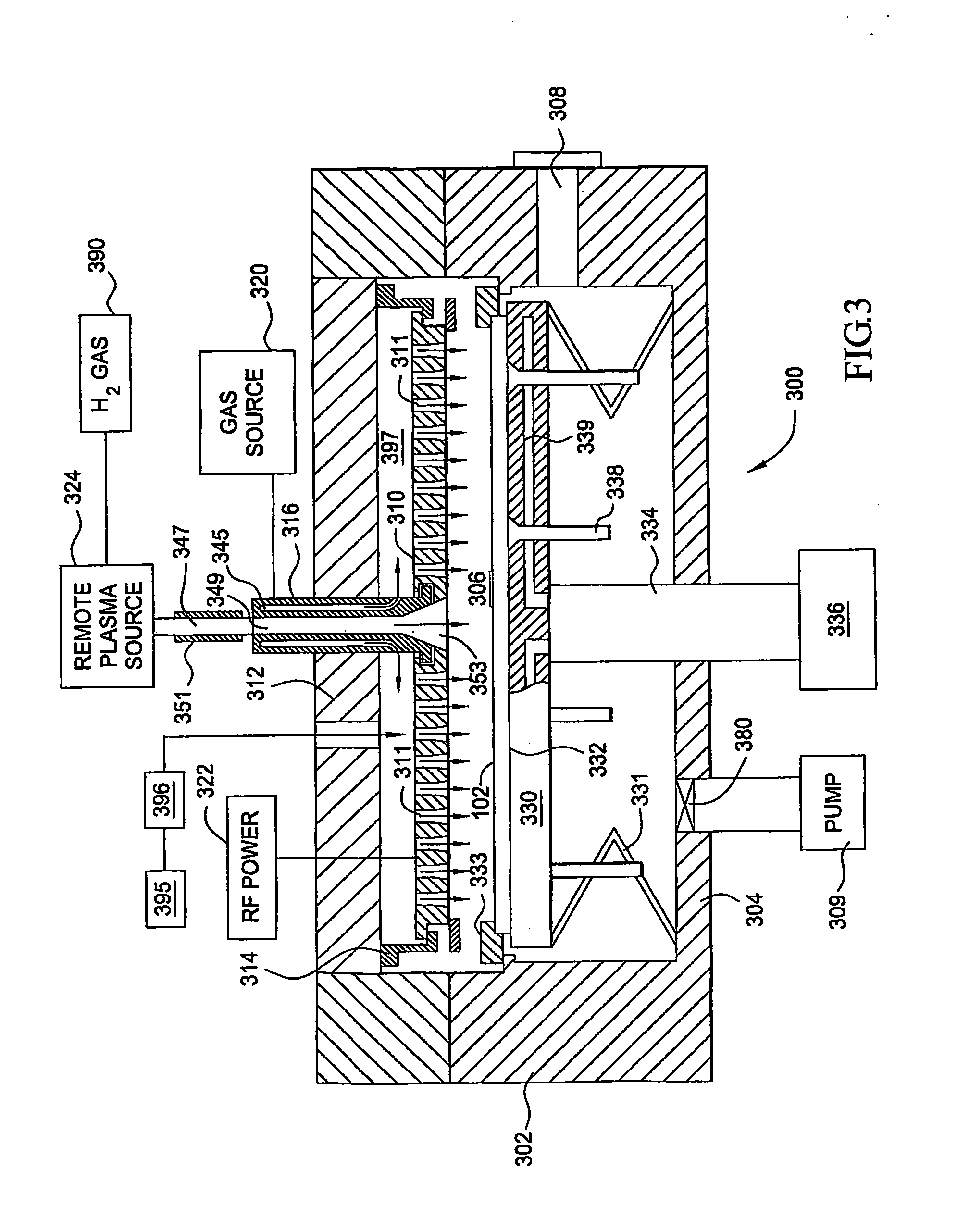
[0018]Embodiments of the present invention generally provide improved apparatus and methods for depositing amorphous and microcrystalline silicon films during the formation of solar cells. In one embodiment, a method and apparatus is provided for generating and introducing hydrogen radicals directly into a processing region of a processing chamber for reaction with a silicon-containing precursor for film deposition on a substrate. In one embodiment, the hydrogen radicals are generated by a remote plasma source and directly introduced into the processing region via a line of sight path to minimize the loss of energy by the hydrogen radicals prior to reaching the processing region. The line of sight path may include tubing formed from a non-reactive material, such as a dielectric or ceramic material. In some configurations, it is desirable to heat the tubing to reduce the possible transfer of energy to the tubing and prevent adsorption of the hydrogen radicals onto the surface of the ...


PUM

PropertyMeasurementUnit
Flow rateaaaaaaaaaa
Chemically inertaaaaaaaaaa

Abstract

An apparatus and methods for depositing amorphous and microcrystalline silicon films during the formation of solar cells are provided. In one embodiment, a method and apparatus is provided for generating and introducing hydrogen radicals directly into a processing region of a processing chamber for reaction with a silicon-containing precursor for film deposition on a substrate. In one embodiment, the hydrogen radicals are generated by a remote plasma source and directly introduced into the processing region via a line of sight path to minimize the loss of energy by the hydrogen radicals prior to reaching the processing region.

Description

BACKGROUND OF THE INVENTION[0001]1. Field of the Invention[0002]Embodiments of the invention relate to an apparatus and method for forming solar cells. More particularly, embodiments of the present invention relate to an apparatus and method for forming amorphous and microcrystalline silicon layers utilized in solar cell applications.[0003]2. Description of the Related Art[0004]Photovoltaic (PV) devices or solar cells are devices which convert sunlight into direct current (DC) electrical power. Typical thin film PV devices, or thin film solar cells, have one or more p-i-n junctions. Each p-i-n junction comprises a p-type layer, an intrinsic type layer, and an n-type layer. When the p-i-n junction of the solar cell is exposed to sunlight (consisting of energy from photons), the sunlight is converted to electricity through the PV effect. Solar cells may be tiled into larger solar arrays.[0005]Typically, a thin film solar cell includes active regions, or photoelectric conversion units,...

Claims


Application Information

Patent Timeline
IPC IPC(8): H01L21/31
CPCC23C16/24C23C16/452C23C16/45514C23C16/45565Y02E10/545C23C16/45574C23C16/5096H01L31/1824H01L31/202C23C16/4557Y02P70/50C23C16/44H01L21/20H01L21/0262
Inventor LAKSHMANAN, ANNAMALAITANG, JIANSHEHO, DUSTIN W.SCHMITT, FRANCIMAR C.TSO, ALANCHO, TOM K.SHIEH, BRIAN SY-YUANPONNEKANTI, HARI K.EBERSPACHER, CHRISYUAN, ZHENG
Owner APPLIED MATERIALS INC
Why Eureka
Try Eureka