Clock domain crossing interface

Active Publication Date: 2013-01-10
PSION
View PDF9 Cites 22 Cited by
  • Summary
  • Abstract
  • Description
  • Claims
  • Application Information

AI Technical Summary

Benefits of technology

[0013]These together with other aspects and advantages which will be subsequently apparent, reside in the details of construction and operation as more fully h

Problems solved by technology

These interfaces must conform to strict design principles for rel

Method used


Image

  • Clock domain crossing interface
  • Clock domain crossing interface
  • Clock domain crossing interface

Examples


Embodiment Construction

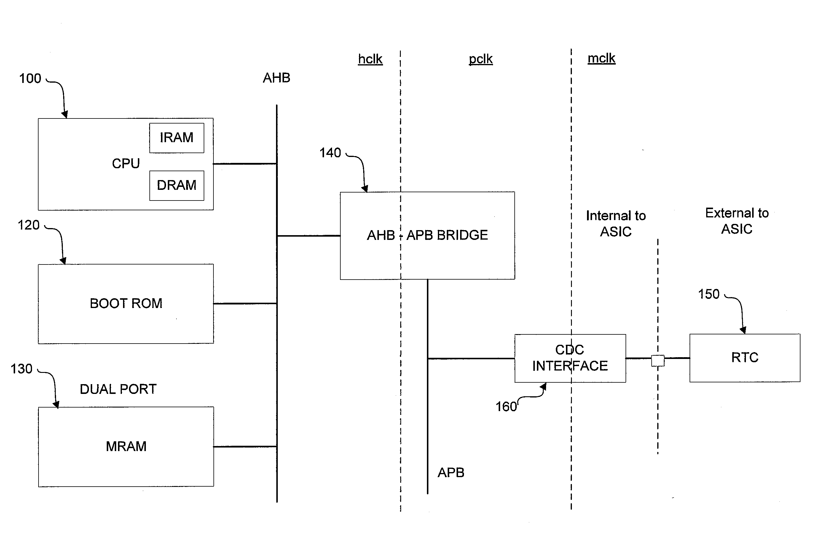
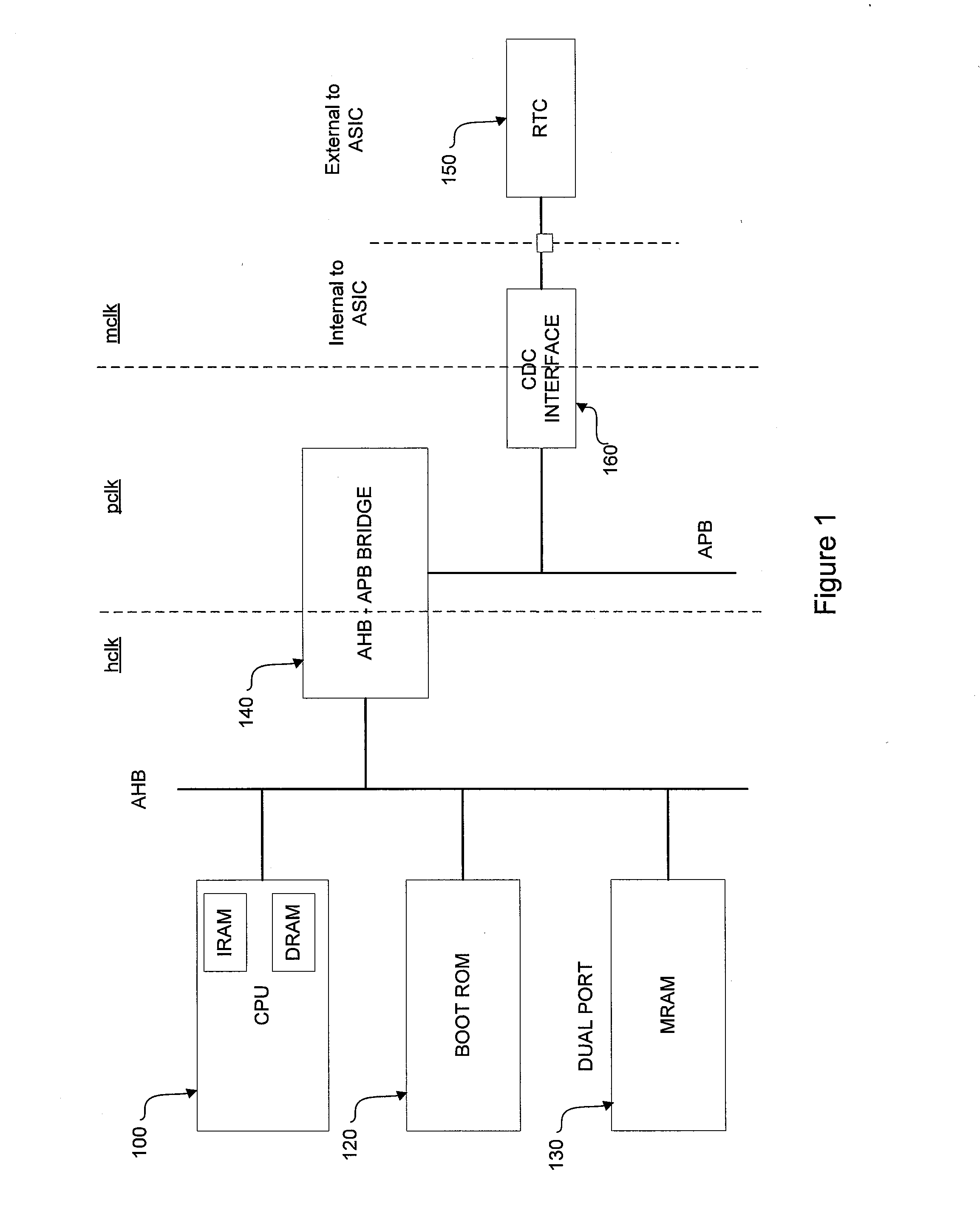
[0022]FIG. 1 is a simplified block diagram of a typical AMBA-based SoC device incorporating the CDC interface of the present invention. A high-performance system backbone bus, AHB, is provided over which a plurality of modules communicate, such as a CPU 100 (e.g. a high performance ARM processor), on-chip messaging memory (MRAM) 120 and a boot ROM 130. The CPU 100 may incorporate tightly-coupled IRAM and DRAM memories. The MRAM 120 is preferably a dual-port memory (i.e. shared across multiple interfaces) that is accessible by an external host processor (not shown). A bus clock signal, hclk provides signal timing for all bus transfers to and from the AHB. According to the AMBA specification, all signal timing on the AHB is related to the rising edge of the hclk clock signal.

[0023]Also located on the high performance AHB is a bridge 140 to a lower bandwidth APB. The APB is designed for controlled access to register interfaces on system peripherals. According to the AMBA specification,...


PUM


Abstract

A flexible and scalable bi-directional CDC interface is set forth between clock domains in a SoC device. The interface comprises a pulse sync circuit for receiving a pulse synchronized to the source clock domain and in response outputting a busy signal to the source clock domain and outputting the pulse synchronized to said destination clock domain; an input register for latching data from said source clock domain in response to a transition of said source clock in the event said busy signal is not active and preventing said data from being latched in the event said busy signal is active so as not to corrupt previously latched data; and an output register for receiving said pulse from said pulse sync circuit and in response latching said pulse from said input register on a transition of said destination clock.

Description

BACKGROUND OF THE INVENTION[0001]1. Field of the Invention[0002]The present invention is directed to bus architectures for System-on-a-Chip (SoC) devices, and more particularly to a clock domain crossing interface for transferring a synchronous clock signal from one clock domain to another clock domain in a SoC device.[0003]2. Description of the Related Art[0004]The term “system-on-a-chip” or SoC commonly refers to an integrated circuit on which all of the necessary electronic circuits and parts are packaged to create a complete “system” (e.g. a hand-held or vehicle-mounted computer, cell phone, digital camera, etc.). Such circuits normally include a microcontroller or microprocessor, memory, timing sources, peripherals and external interfaces to analog and / or digital devices. These components are interconnected by a plurality of busses, such as those defined in the Advanced Microcontroller Bus Architecture (AMBA), developed by ARM Ltd. AMBA defines specifications for the busses use...

Claims


Application Information

Patent Timeline
IPC IPC(8): G06F1/12
CPCH04L7/02G06F5/10H04L7/005G06F1/12G06F2205/102
Inventor MADDIGAN, STEVEN WILLIAMEPASSA HABIB, DIMITRI GABRIEL
Owner PSION
Why Eureka
Try Eureka