Semiconductor device with field threshold MOSFET for high voltage termination

Active Publication Date: 2013-01-24
ALPHA & OMEGA SEMICON INC
View PDF8 Cites 52 Cited by
  • Summary
  • Abstract
  • Description
  • Claims
  • Application Information

AI Technical Summary

Benefits of technology

[0011]It is therefore an aspect of the present invention to provide a new and improved edge termination configuration to reduce the electrical field crowding effects near the blocking junction at the device edge and provide a compact termination with lower surface electric field that is less sensitive to surface charge. This is achieved with the formation of a plurality of P-channel MOSFETs in the N region and between two P-type diffusion regions or between two floating guard rings (FGRs). In one embodiment, a poly silicon or metal layer covering an oxide layer are deposited at the region between the FGRs. This p

Problems solved by technology

Conventional floating guard rings in the termination area are not reliable especially products housed in plastic packages due to spacing of the Floating Guard Rings (FGR) and the charge from dielectric layer under the metal layer, passivation film, and/or char

Method used


Image

  • Semiconductor device with field threshold MOSFET for high voltage termination
  • Semiconductor device with field threshold MOSFET for high voltage termination
  • Semiconductor device with field threshold MOSFET for high voltage termination

Examples


first embodiment

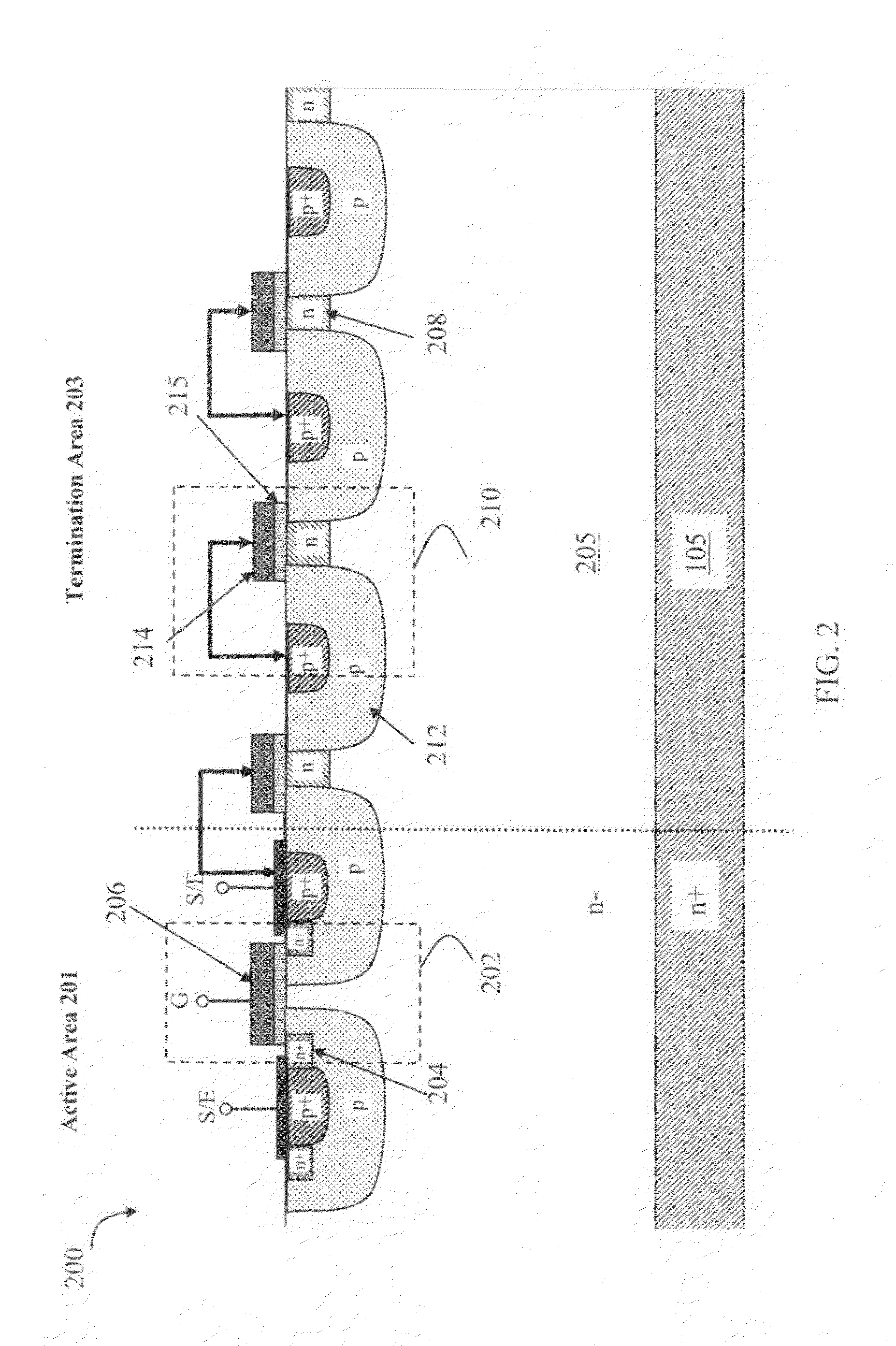
[0023]FIG. 2 is a cross-sectional view of a planar gate HV device 200 of the type depicted in FIG. 1 along line A-A according to the present invention. The HV device 200 is formed on a semiconductor substrate including a lightly doped N-type layer 205 supported on top of a heavily doped layer 105. The doping polarities of heavily doped layer 105 and the lightly doped layer 205 are the same for a HV MOSFET device and are opposite for a HV IGBT device. For simplicity the description in this application only illustrates a HV MOSFET device. The HV device 200 includes an active area 201 and a termination area 203. The active area 201 includes a plurality of planar gate N-channel vertical MOSFETs 202, each of which includes an n+ source 204, a drain formed in the n+ substrate 105 and a planar gate 206. The termination area 203 includes a plurality of P-channel MOSFETs 210, each of which locates between two P-type diffusion regions or two floating guard rings (FGRs) 212. The P-type floatin...

second embodiment

[0026]FIG. 4 is a cross-sectional view illustrating a trench gate high voltage (HV) device 400 according to the present invention. The active area 401 of the device 400 includes a plurality of trench gate vertical N-channel MOSFETs 402, each of which includes an n+ source 404, a trench gate 406 and a drain formed in the n+ substrate 105. Similar to device 200 of FIG. 2, the termination area 403 of the device 400 includes a plurality of P-channel planar gate lateral MOSFETs 210, each of which locates between two P-type diffusion regions or between two FGRs 212, with the gate 214 connecting to the drain electrode 212. The P-channel MOSFET transistors 210 act as a chain between the active area and the scribe region (die edge) in a cascade fashion as described above. The FGR 212 may be formed at the same time the P body region of the active transistor is formed with the same dopant density. Alternatively, the termination area 403 can includes a plurality of P-channel MOSFETs 211 as show...

third embodiment

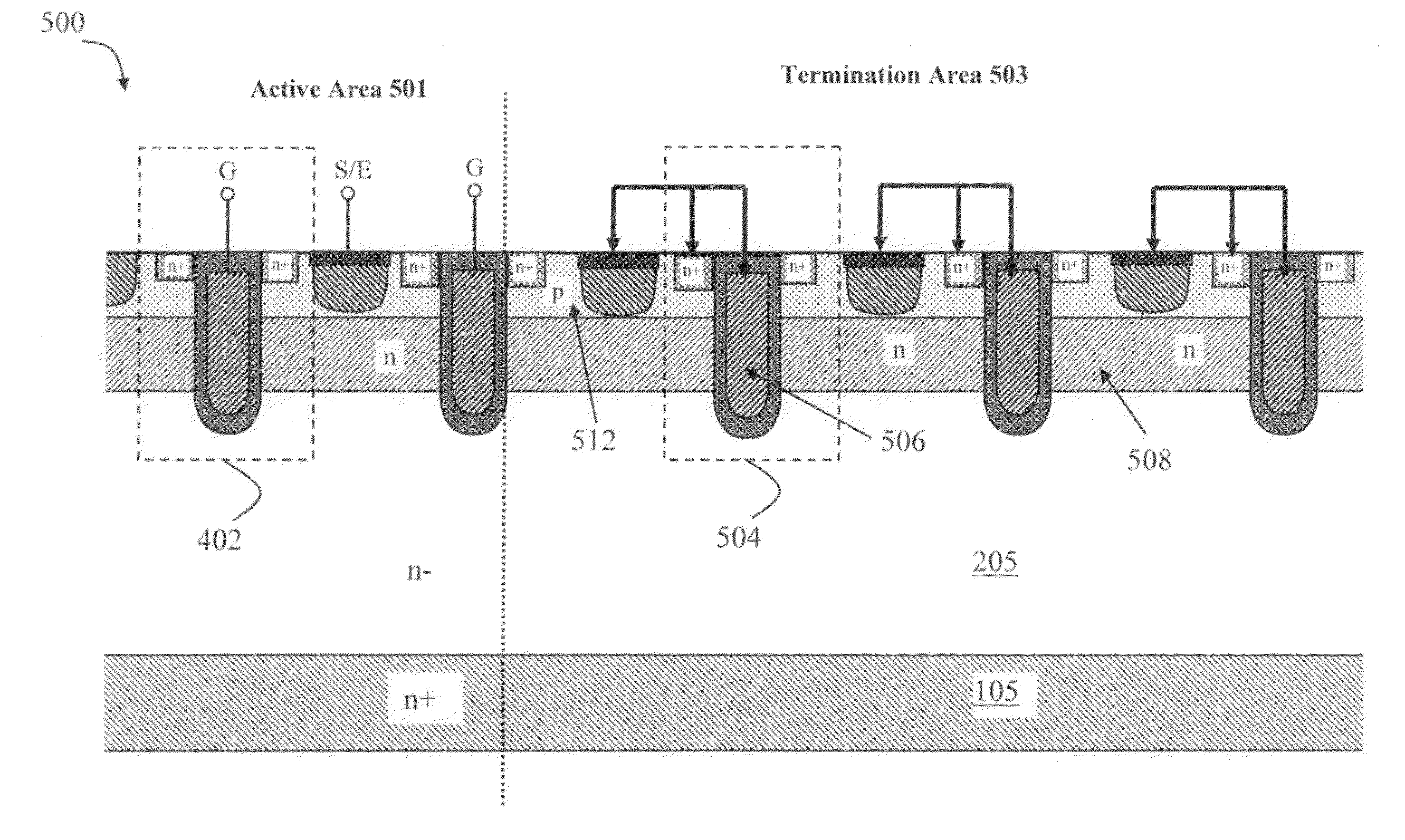
[0027]FIG. 5 is a cross-section view illustrating another trench gate HV device 500 according to the present invention. In this embodiment, the active area 501 includes a plurality of trench gate vertical N-channel MOSFETs 402 of the type depicted in FIG. 4. The termination area 503 includes a plurality of trench gate P-channel lateral MOSFETs 504, each of which has the same structure as the trench gate MOSFET 402 and locates between two P-type diffusion regions or two FGRs 512. The plurality of termination trenches are formed to have a distance ranging from 0.5 to 5 microns between two adjacent termination trenches and a depth into the semiconductor substrate ranging from 0.5 to 8 microns. The gate material 506 of each P-channel MOSFET 504 functions as a trench gate and is connected to a drain electrode 512 (Drain of the Trench MOSFET is the p-region with more negative Potential). Each FGR 512 between two trench gate 506 in termination area 503 functions as the drain of one P-chann...


PUM


Abstract

This invention discloses a semiconductor power device disposed in a semiconductor substrate comprising a lightly doped layer formed on a heavily doped layer and having an active cell area and an edge termination area. The edge termination area comprises a plurality P-channel MOSFETs. By connecting the gate to the drain electrode, the P-channel MOSFET transistors formed on the edge termination are sequentially turned on when the applied voltage is equal to or greater than the threshold voltage Vt of the P-channel MOSFET transistors, thereby optimizing the voltage blocked by each region.

Description

BACKGROUND OF THE INVENTION[0001]1. Field of the Invention[0002]The invention relates generally to the semiconductor power devices. More particularly, this invention relates to configurations and methods for manufacturing of new and improved edge terminations for high voltage (HV) devices for improved reliability and to reduce the areas occupied by the termination areas while maintaining high breakdown voltages.[0003]2. Description of the Prior Art[0004]Conventional floating guard rings in the termination area are not reliable especially products housed in plastic packages due to spacing of the Floating Guard Rings (FGR) and the charge from dielectric layer under the metal layer, passivation film, and / or charge from the plastic molding compounds. Other high voltage (higher than 400V) termination structures, such as Junction Termination Extension (JTE), Field Guard Ring and Field Plate (FGR-FP), minimize sensitivity of FGR type high voltage (HV) termination.[0005]“Optimization and Su...

Claims


Application Information

Patent Timeline
IPC IPC(8): H01L27/088H01L21/8234
CPCH01L27/088H01L29/404H01L29/7803H01L29/0878H01L29/7813H01L29/0619H01L29/0638H01L29/7811
Inventor YILMAZ, HAMZABOBDE, MADHUR
Owner ALPHA & OMEGA SEMICON INC
Why Eureka
Try Eureka