

Thin film manufacturing apparatus, thin film manufacturing method and method for manufacturing semiconductor device
a technology of thin film and manufacturing method, which is applied in the direction of liquid surface applicators, coatings, chemical vapor deposition coatings, etc., can solve the problems of changing the temperature of the entire film manufacturing apparatus never uniformly reaches a predetermined level, and the difficulty in controlling the temperature of the substrate, so as to reduce the fluctuations of the substrate temperature encountered, reduce the fluctuations of the substrate temperature, and reduce the effect of temperature control
- Summary
- Abstract
- Description
- Claims
- Application Information
AI Technical Summary
Benefits of technology
Problems solved by technology
Method used
Image

Examples
Embodiment Construction
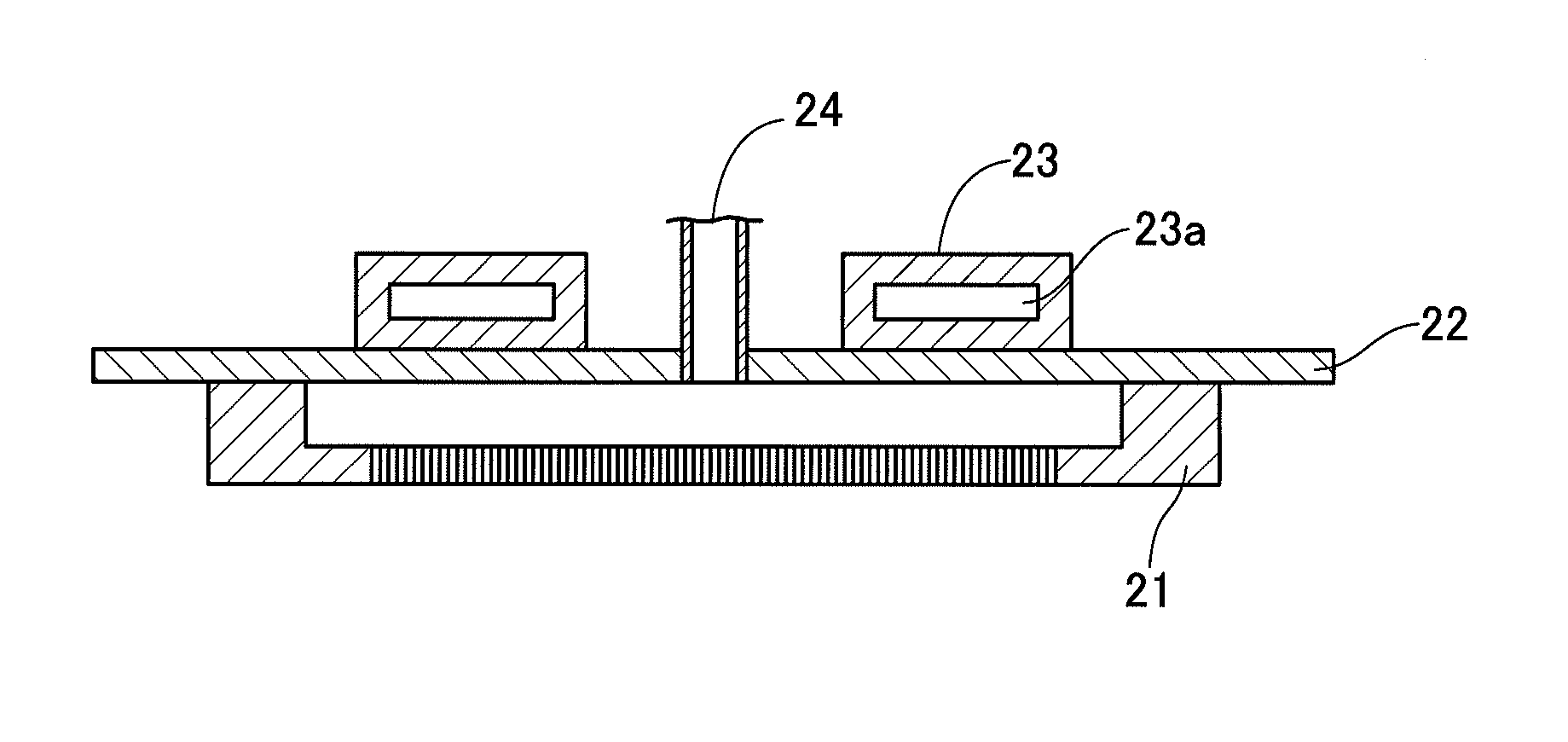
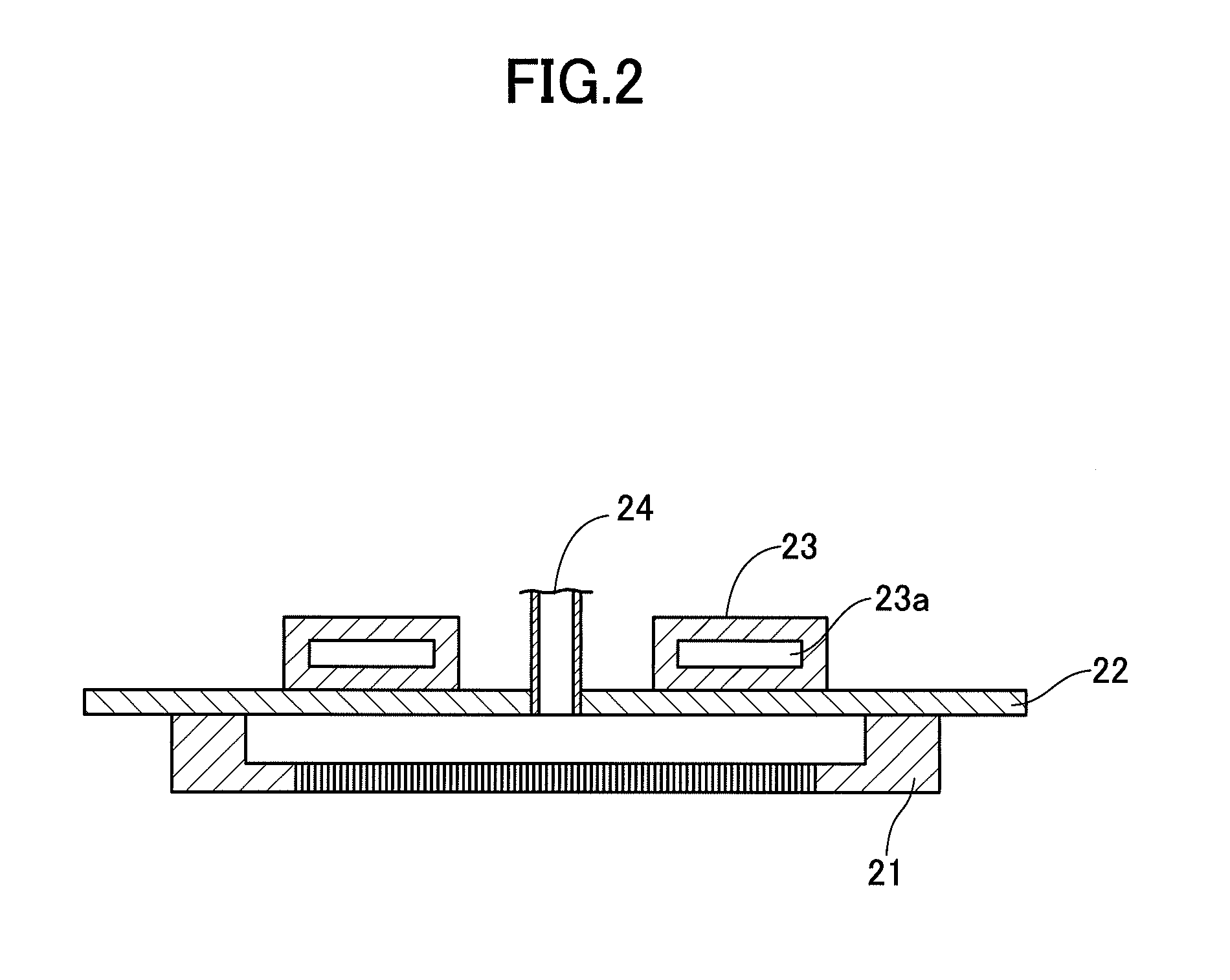
[0047]According to an embodiment of the thin film manufacturing apparatus relating to the present invention, there is provided an apparatus for forming a ceramic thin film according to the thermal CVD technique such as the MOCVD technique, wherein the apparatus is provided with internal jigs such as one of a shower plate and a part for mounting or securing a shower plate or both of a shower plate and a part for mounting or securing a shower plate, which are covered with a film of a heat radiation material on the surface thereof, at a position facing the substrate on which a desired film is to be deposited or a position on the side of the gas-introduction port of the substrate, wherein the internal jig is, if necessary, provided with a heating mechanism or a heat-exchangeable jig through which a liquid heating medium is circulated, in such a manner that the heating mechanism or the heat-exchangeable jig comes in close contact with the internal jig and wherein a thermocouple for deter...
PUM
| Property | Measurement | Unit |
|---|---|---|
| Temperature | aaaaa | aaaaa |
| Temperature | aaaaa | aaaaa |
| Ferroelectricity | aaaaa | aaaaa |
Abstract
Description
Claims
Application Information