
N-channel and p-channel finfet cell architecture with inter-block insulator

a cell architecture and inter-block insulator technology, applied in the field of n-, can solve the problems of compromising the reliability of polysilicon gate traces traversing the inter-block insulator, affecting the reliability of polysilicon gate traces, and increasing the requirements of low power and compact layout,

Active Publication Date: 2013-01-31
SYNOPSYS INC
View PDF3 Cites 94 Cited by
  • Summary
  • Abstract
  • Description
  • Claims
  • Application Information

AI Technical Summary

Benefits of technology

The patent describes a method for designing structures using finFET technology to create a wide variety of cells for integrated circuits. It also describes creating libraries of these cells for use in design automation software. The creation of these libraries helps in reducing the time and effort required for designing complex circuits. The technical effects of this patent are improved efficiency and flexibility in designing finFET block structures for integrated circuits.

Problems solved by technology

FinFETs have gained acceptance recently as the requirements of low power and compact layout have become more demanding.
For FinFET blocks, the channels of the transistors comprise narrow fins, that can be susceptible to warping or other distortion when formed in regions of unbalanced stress, such as can occur at the edges adjacent the inter-block insulators.
Also, for smaller feature sizes, the reliability of polysilicon gate traces traversing the inter-block insulators can be compromised by the non-uniformity of the structures.

Method used


Image

  • N-channel and p-channel finfet cell architecture with inter-block insulator
  • N-channel and p-channel finfet cell architecture with inter-block insulator
  • N-channel and p-channel finfet cell architecture with inter-block insulator

Examples


Embodiment Construction

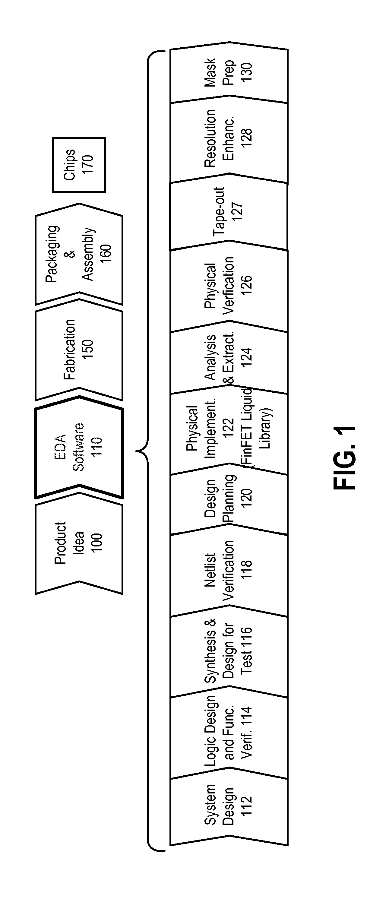
[0020]FIG. 1 is a simplified representation of an integrated circuit design flow. As with all flowcharts herein, it will be appreciated that many of the steps of FIG. 1 can be combined, performed in parallel or performed in a different sequence without affecting the functions achieved. In some cases a rearrangement of steps will achieve the same results only if certain other changes are made as well, and in other cases a rearrangement of steps will achieve the same results only if certain conditions are satisfied. Such rearrangement possibilities will be apparent to the reader.

[0021]At a high level, the process of FIG. 1 starts with the product idea (block 100) and is realized in an EDA (Electronic Design Automation) software design process (block 110). When the design is finalized, the fabrication process (block 150) and packaging and assembly processes (block 160) occur, ultimately resulting in finished integrated circuit chips (result 170).

[0022]The EDA software design process (b...


PUM


Abstract

A finFET block architecture includes a first set of semiconductor fins having a first conductivity type, and a second set of semiconductor fins having a second conductivity type. An inter-block insulator is placed between outer fins of the first and second sets. A patterned gate conductor layer includes a first plurality of gate traces extending across the set of fins in the first block without crossing the inter-block insulator, and a second plurality of gate traces extending across the set of fins in the second block without crossing the inter-block insulator. Patterned conductor layers over the gate conductor layer are arranged in orthogonal layout patterns, and include an inter-block connector arranged to connect gate traces in the first and second blocks.

Description

BACKGROUND[0001]1. Field of the Invention[0002]The present invention relates to integrated circuit devices, cell libraries, cell architectures and electronic design automation tools for integrated circuit devices, including finFET devices.[0003]2. Description of Related Art[0004]FinFET style transistors have been described in D. Hisamoto et al., IEDM, 1998; and N. Lindert et al., IEEE Electron Device Letters, p. 487, 2001. FinFETs have gained acceptance recently as the requirements of low power and compact layout have become more demanding. In CMOS devices, N-type and P-type blocks of transistors are placed in proximity, with insulators in between to prevent latch up, and other problems.[0005]In the design of integrated circuits, standard cell libraries are often utilized. It is desirable to provide a finFET-based design architecture suitable for implementation of cells for a standard cell library, and for implementation of integrated circuits using finFET architectures with flexibl...

Claims


Application Information

Patent Timeline
IPC IPC(8): H01L27/12H01L21/82G06F17/50
CPCH01L27/0207H01L27/0924H01L27/0886G06F17/5068G06F17/5072H01L27/1211G06F30/39H01L2924/0002H01L2924/00G06F30/327G06F30/392G06F30/394G06F30/398H01L23/528
Inventor KAWA, JAMILMOROZ, VICTORSHERLEKAR, DEEPAK
Owner SYNOPSYS INC
Features
  • Generate Ideas
  • Intellectual Property
  • Life Sciences
  • Materials
  • Tech Scout
  • Unparalleled Data Quality
  • Higher Quality Content
  • 60% Fewer Hallucinations
Learn More