Method of forming microstructure, laser irradiation device, and substrate

a technology of laser irradiation and microstructure, which is applied in the direction of printing element electric connection formation, manufacturing tools, etc., can solve the problems of excessive etching speed, non-modified region etching at which the laser has not been irradiated, and different ease of etching, so as to improve adhesion and smooth flow through the fluid channel

Inactive Publication Date: 2013-01-31
THE FUJIKURA CABLE WORKS LTD
View PDF4 Cites 21 Cited by
  • Summary
  • Abstract
  • Description
  • Claims
  • Application Information

AI Technical Summary

Benefits of technology

[0018]According to the method of forming a microstructure according to an aspect of the present invention, the laser irradiation is performed while keeping the orientation of the linear polarization of the laser beam in a certain direction with respect to the scanning direction of the laser beam. Thereby, it is possible to form easy to etch areas and hard to etch areas in a certain direction, alternating with respect to the scanning direction. That is to say, the easy to etch areas and hard to etch areas are formed in the same state at any position regardless of the position at which the modified region is formed in the substrate. That is to say, the ease of etching is of the same extent. For this reason, it is possible to form a microstructure at nearly a constant etching speed without being influenced by the arrangement or shape of the modified region in the substrate. Therefore, it is possible to accurately control the size of a microstructure such as a micro hole or the like.
[0029]In accordance with the object, it is possible to cause various fluids to flow in the micro hole in a substrate that has the micro hole. For example, using the substrate as an interconnection substrate, a coolant such as air or water is circulated in this micro hole (fluidic channel). At this time, by this cooling function, it is possible to effectively lower the temperature rise of the substrate even when a device with a large heat value is mounted on this interconnection substrate. In addition, the substrate is used as a substrate that integrates a bio test system using micro-fluidics technology. In this case, it is possible to apply this micro hole (fluidic channel) to a fluidic channel that circulates biopolymer solutions, such as DNA (nucleic acid), protein materials, and lipids.

Problems solved by technology

In the conventional method, when removing modified regions from a substrate by wet etching, even when the shapes of the modified regions have comparable complexity, there has been the problem of the ease of etching (etching speed) differing among micro holes whose placement differs in the substrate.
For this reason, there has been the problem in which, by the time the etching of the modified region 103 is completed, etching of a non-modified region at which the laser has not been irradiated has excessively advanced.

Method used


Image

  • Method of forming microstructure, laser irradiation device, and substrate
  • Method of forming microstructure, laser irradiation device, and substrate
  • Method of forming microstructure, laser irradiation device, and substrate

Examples


first embodiment

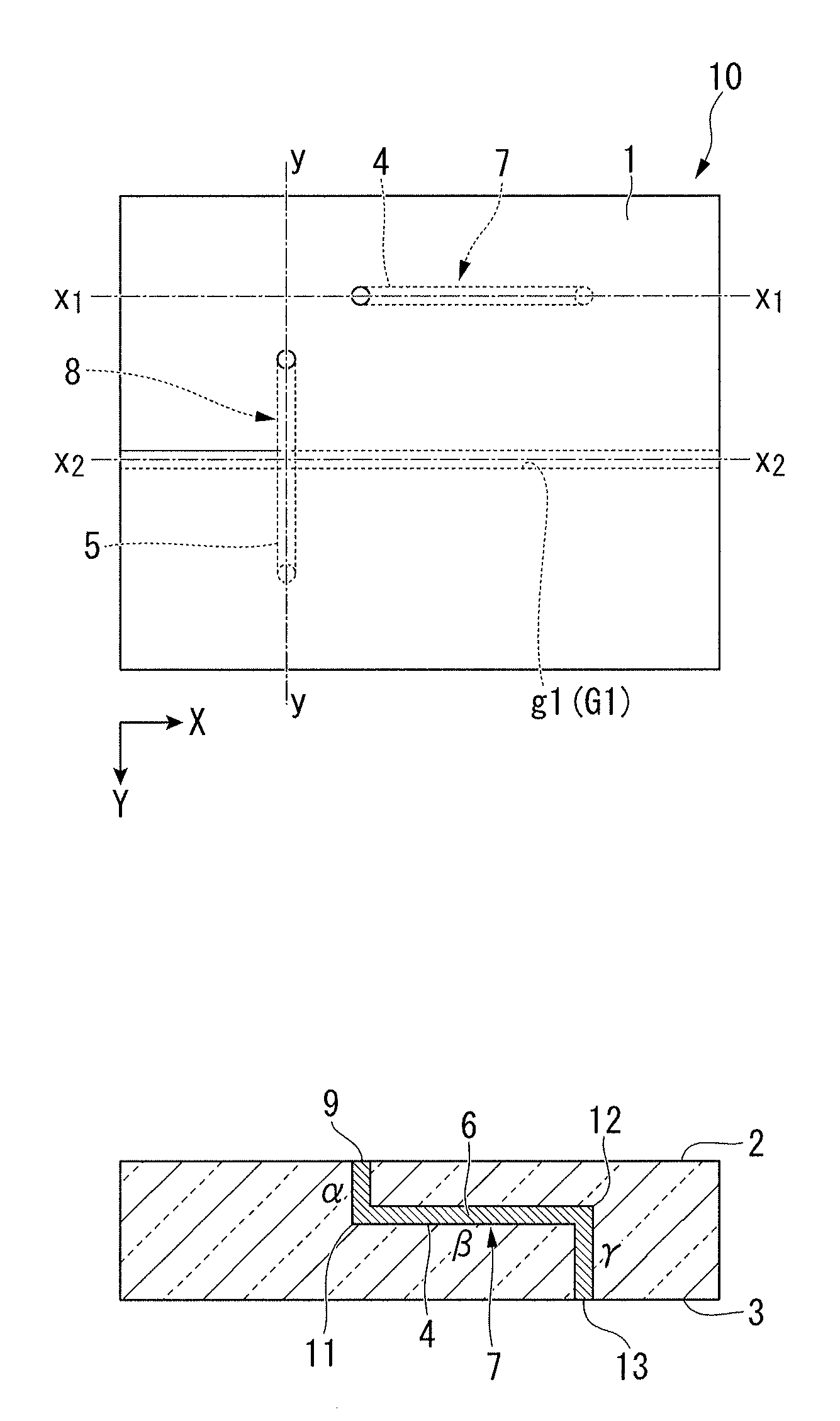
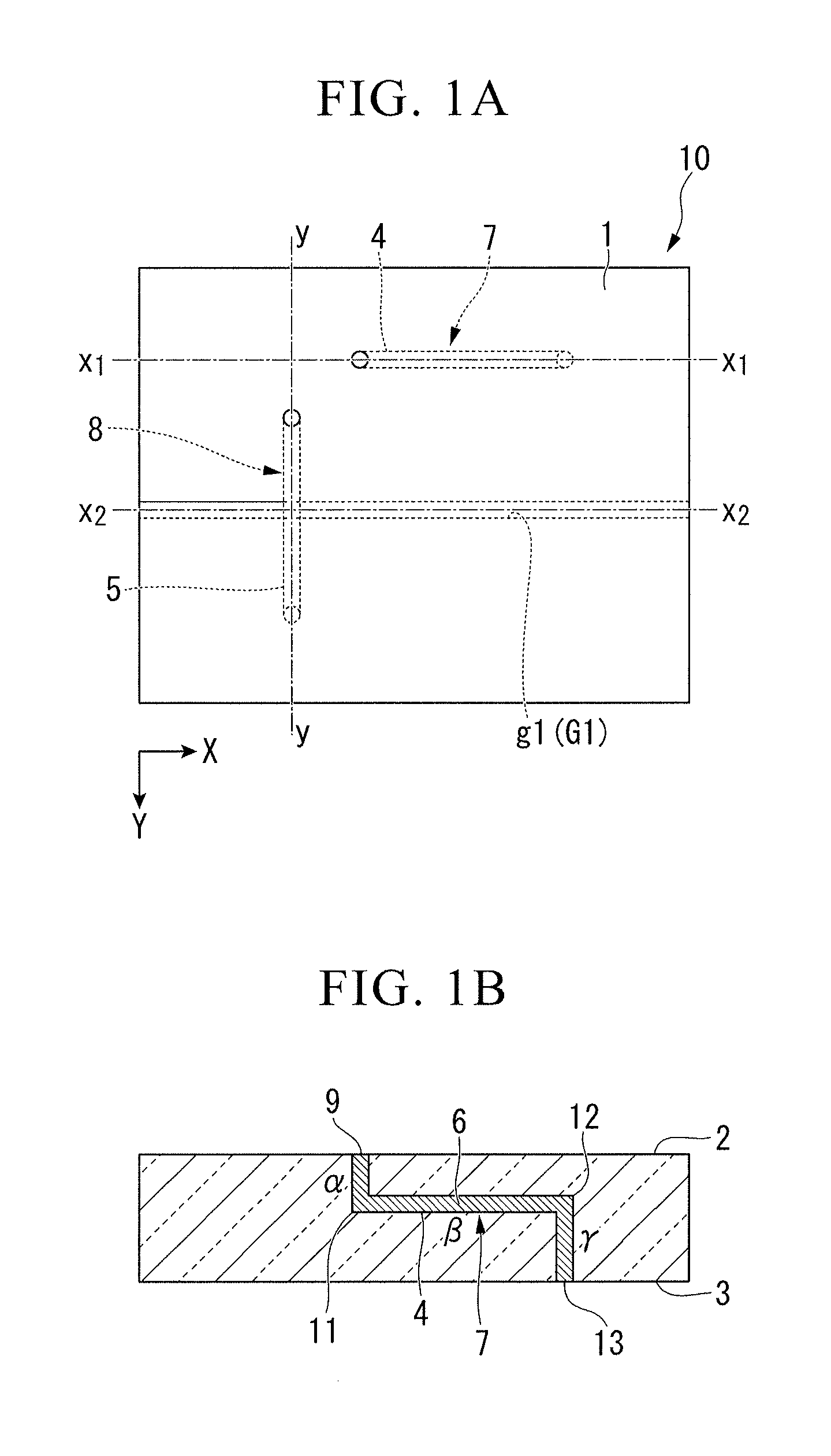
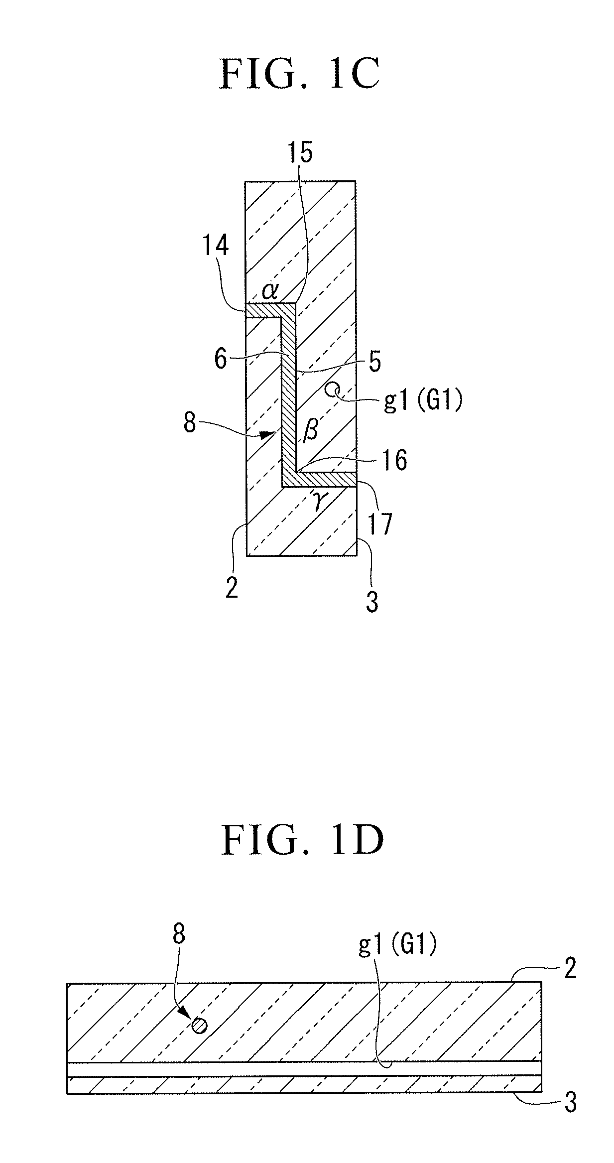
Interposer Substrate 10

[0106]FIG. 1A is a plan view of the interposer substrate 10 according to the first embodiment of the present invention. FIG. 1B is a cross-sectional view along line x1-x1 of FIG. 1A. FIG. 1C is a cross-sectional view along line y-y of FIG. 1A. FIG. 1D is a cross-sectional view along line x2-x2 of FIG. 1A.

[0107]This interposer substrate 10 is provided with a first through-hole interconnection 7 and a second through-hole interconnection 8 that are formed by arranging a first micro hole 4 and a second micro hole 5 so as to connect one principal surface 2 (first principal surface) and another principal surface 3 (second principal surface) that constitute a substrate 1 and filling or forming a conductive substance 6 in each micro hole.

[0108]The first through-hole interconnection 7 is provided with a region a that extends in the thickness direction of the substrate 1 from an opening portion 9 that appears at the one principal surface 2 to a bend portion 11, a region...

second embodiment

Surface Interconnection Substrate 30

[0118]FIG. 2A is a plan view of a surface interconnection substrate 30 according to the second embodiment of the present invention. FIG. 2B is a cross-sectional view along line x1-x1 of FIG. 2A. FIG. 2C is a cross-sectional view along line y1-y1 of FIG. 2A. FIG. 2D is a cross-sectional view along line x2-x2 of FIG. 2A. FIG. 2E is a cross-sectional view along line y2-y2 of FIG. 2A.

[0119]This surface interconnection substrate 30 is provided with a first surface interconnection 37 that is formed by a first micro groove 34 being formed in the surface of one principal surface 32 (first principal surface) that constitutes a substrate 31, and filling or forming a conductive substance 36 in this micro groove 34. Moreover, a first fluidic channel G2 that consists of a first micro hole g2, and a second fluidic channel G3 that consists of a second micro hole g3 are provided in the surface interconnection substrate 30.

[0120]The first surface interconnection 3...


PUM

PropertyMeasurementUnit
thicknessaaaaaaaaaa
sizesaaaaaaaaaa
sizeaaaaaaaaaa

Abstract

A method of forming a microstructure includes a Step (A) of forming a modified region in a substrate by irradiating a laser beam having a pulse duration on the order of picoseconds or shorter on a region where a pore-like microstructure is to be provided, and scanning a focal point at which the laser beam is converged; and a Step (B) of forming a microstructure by performing an etching process on the substrate in which the modified region has been formed, and removing the modified region, where a linear polarized laser beam is used as the laser beam in the Step (A), and the laser beam is irradiated so that an orientation of a linear polarization has a certain direction with respect to a direction of scanning the focal point.

Description

CROSS REFERENCE TO RELATED APPLICATIONS[0001]This application is a continuation application based on a PCT Patent Application[0002]No. PCT / JP2011 / 058033, filed Mar. 30, 2011, whose priority is claimed on Japanese Patent Application No. 2010-089509 filed Apr. 8, 2010, the entire content of which are hereby incorporated by reference.BACKGROUND OF THE INVENTION[0003]1. Field of the Invention[0004]The present invention relates to a method of a forming microstructure in a substrate using a laser beam, a laser irradiation device that is used in this method, a substrate that is manufactured using this method and a substrate having a micro hole. More particularly, it relates to a method of forming a micro hole in a substrate using a laser beam, a laser irradiation device that is used in this method, and a substrate that is manufactured using this method and a substrate that has a micro hole.[0005]2. Description of the Related Art[0006]Conventionally, as a method of electrically connecting a...

Claims


Application Information

Patent Timeline
Patent Type & Authority Applications(United States)
IPC IPC(8): B29C59/16B32B3/24B44C1/22B23K26/00B23K26/046B23K26/36H01L23/15H01L23/52H05K3/00H05K3/40
CPCB23K26/0042B23K26/0635H01L21/4803H01L21/4846H01L23/473Y10T428/24273H05K2203/107B23K26/365H01L2924/0002H05K3/002H01L2924/00B23K26/0006B23K26/0624B23K26/361B23K2103/56
Inventor WAKIOKA, HIROYUKI
Owner THE FUJIKURA CABLE WORKS LTD
Why Eureka
Try Eureka