Critical path delay prediction

a critical path delay and prediction technology, applied in the field of semiconductor chip and integrated circuit technology, can solve the problems of increasing the power demand of semiconductor chips, becoming more difficult to overcome, and proving difficult to achiev

Inactive Publication Date: 2013-02-14
IBM CORP
View PDF26 Cites 7 Cited by
  • Summary
  • Abstract
  • Description
  • Claims
  • Application Information

AI Technical Summary

Problems solved by technology

The increased power demands of semiconductor chips are becoming more difficult to overcome, particularly as chip densities increase.
Unfortunately, efficient use of AVS requires accurate predictions of critical path performance, and particularly critical path delay, something that has proven difficult to achieve.

Method used


Image

  • Critical path delay prediction
  • Critical path delay prediction
  • Critical path delay prediction

Examples


Embodiment Construction

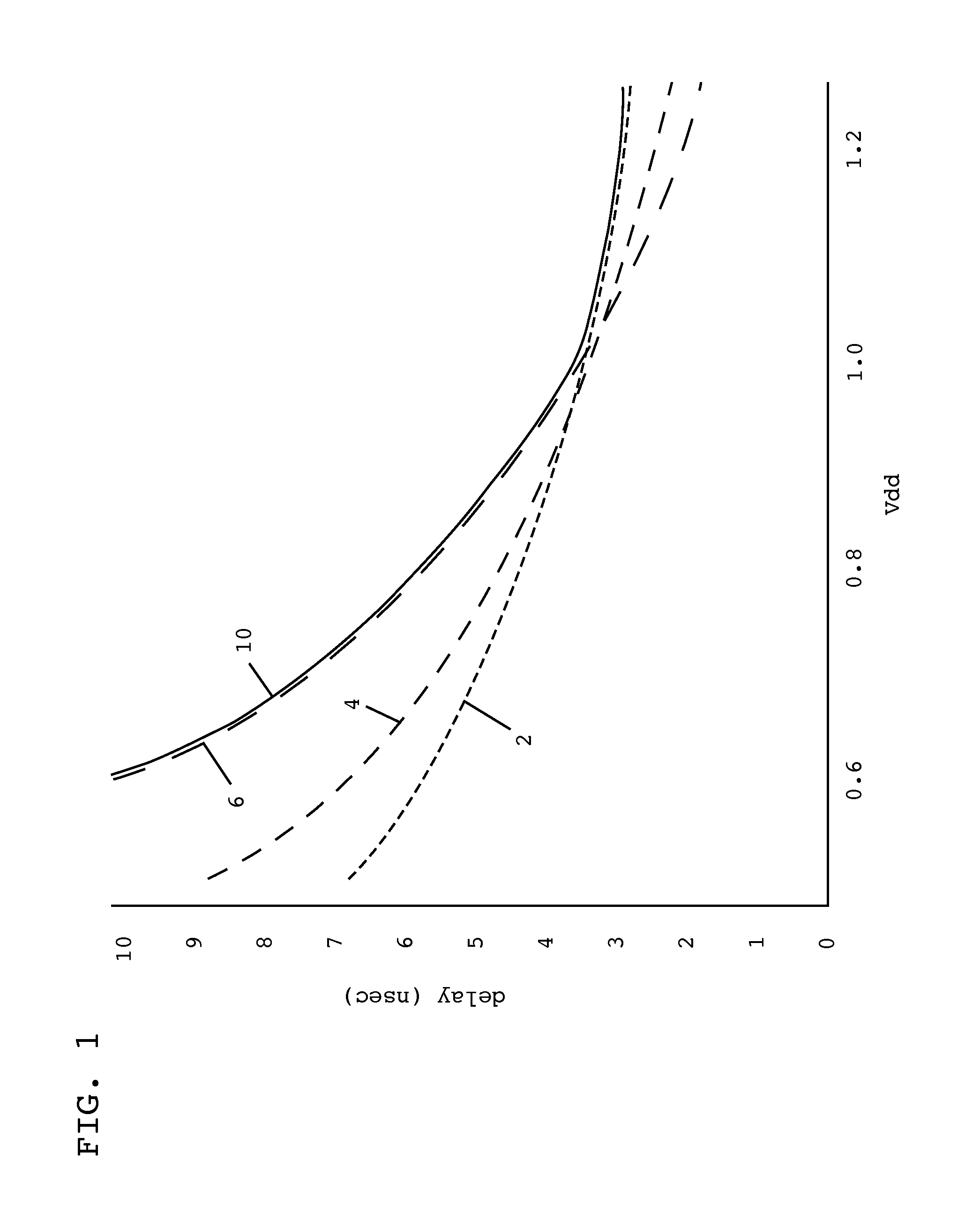
[0014]Turning now to the drawings, FIG. 1 shows an illustrative plot of the delay (in nanoseconds) associated with various critical path components as a function of drain voltage (Vdd). As can be seen in FIG. 1, at drain voltages less than about 1.0, high-voltage threshold (HVT) components 6 exhibit a greater delay than medium-voltage threshold (SVT) components 4 or low-voltage threshold (UVT) components 2. At drain voltages greater than about 1.0, however, UVT components 2 exhibit a greater delay than SVT components 4 or HVT components 6. One difficulty in predicting performance of a critical path, then, and particularly in predicting a delay of a critical path, is the differences in delays attributable to HVT, SVT, and UVT components as drain voltage changes. That is, any predicted delay of a critical path should remain below an upper bound 10 of the delays of all components in order to be useful in maximizing chip efficiency, particularly the efficiencies afforded by adaptive vol...


PUM


Abstract

Embodiments of the invention provide a method, system, and program product for predicting a delay of a critical path. In one embodiment, the invention provides a method of predicting a delay of at least one critical path of an integrated circuit, the method comprising: determining a delay of at least one ring oscillator on the integrated circuit; and calculating a predicted delay for the at least one critical path delay based on a delay of components of the critical path at a corner condition, a wire delay of the at least one critical path, a delay of the at least one ring oscillator at a corner condition, and the determined delay of the at least one ring oscillator.

Description

TECHNICAL FIELD[0001]The present invention relates generally to semiconductor chip and integrated circuit technologies and, more particularly, to the prediction of a critical path delay.BACKGROUND OF THE INVENTION[0002]The increased power demands of semiconductor chips are becoming more difficult to overcome, particularly as chip densities increase. Adaptive voltage scaling (AVS) is one technique used to reduce power consumption. Unfortunately, efficient use of AVS requires accurate predictions of critical path performance, and particularly critical path delay, something that has proven difficult to achieve.SUMMARY OF THE INVENTION[0003]Embodiments of the invention provide methods, systems, and program products for predicting a critical path delay.[0004]A first aspect of the invention provides a method of predicting a delay of at least one critical path of an integrated circuit, the method comprising: determining a delay of at least one ring oscillator on the integrated circuit; and...

Claims


Application Information

Patent Timeline
Patent Type & Authority Applications(United States)
IPC IPC(8): G06F19/00
CPCG06F17/5031G06F30/3312
Inventor CHARLEBOIS, MARGARET R.CHATTY, RASHMI D.HANUDEL, CHRISTOPHER D.HERZL, ROBERT D.MILTON, DAVID W.OGILVIE, CLARENCE R.SZAFIR, MATTHEW P.WILDER, TAD J.
Owner IBM CORP
Why Eureka
Try Eureka