Compensation Circuit of Organic Light Emitting Diode

a light-emitting diode and compensation circuit technology, applied in the direction of lighting devices, instruments, light sources, etc., can solve the problems of increasing the cross voltage of the oled, and affecting the brightness stability of the oled

Active Publication Date: 2013-02-21
HANNSTAR DISPLAY CORPORATION
View PDF3 Cites 28 Cited by
  • Summary
  • Abstract
  • Description
  • Claims
  • Application Information

AI Technical Summary

Benefits of technology

[0018]In summation, the compensation circuit of an organic light emitting diode of the present invention uses the voltage at the node of the control circuit to drop the light emitting efficiency of the organic light emitting diode, and uses the compensation circuit to increase the IOLED to provide a brighter OLED component and achieve the compensation effect, so as to maintain the brightness stability of the OLED.

Problems solved by technology

Since the brightness of the organic light emitting diode (OLED) components depends on the magnitude of current, it is necessary to control the current accurately in order to control pixel brightness accurately, thus incurring a much higher level of difficulty than the conventional TFT-LCD that controls the pixel brightness by controlling the voltage level of writing in pixels only.
In fact, the AMOLED also encounters many problems.
Due to the ageing and deterioration of the OLED, the cross voltage of the OLED will rise and the light emitting efficiency of the OLED will drop gradually after a long time of operation.
The rising cross voltage of the OLED may affect the operation of the thin film transistor.
As to the light emitting efficiency, a long-time operation will cause the ageing and deterioration of the light emitting efficiency.
The drop of the light emitting efficiency for three colors such as red (R), green (G) and blue (B) is different from one another, so that a color shift issue arises, and this problem is not a problem that cannot be solved easily, since the material cannot be improved easily.
As a result, the uniform brightness of the panel will be affected.

Method used


Image

  • Compensation Circuit of Organic Light Emitting Diode
  • Compensation Circuit of Organic Light Emitting Diode
  • Compensation Circuit of Organic Light Emitting Diode

Examples


Embodiment Construction

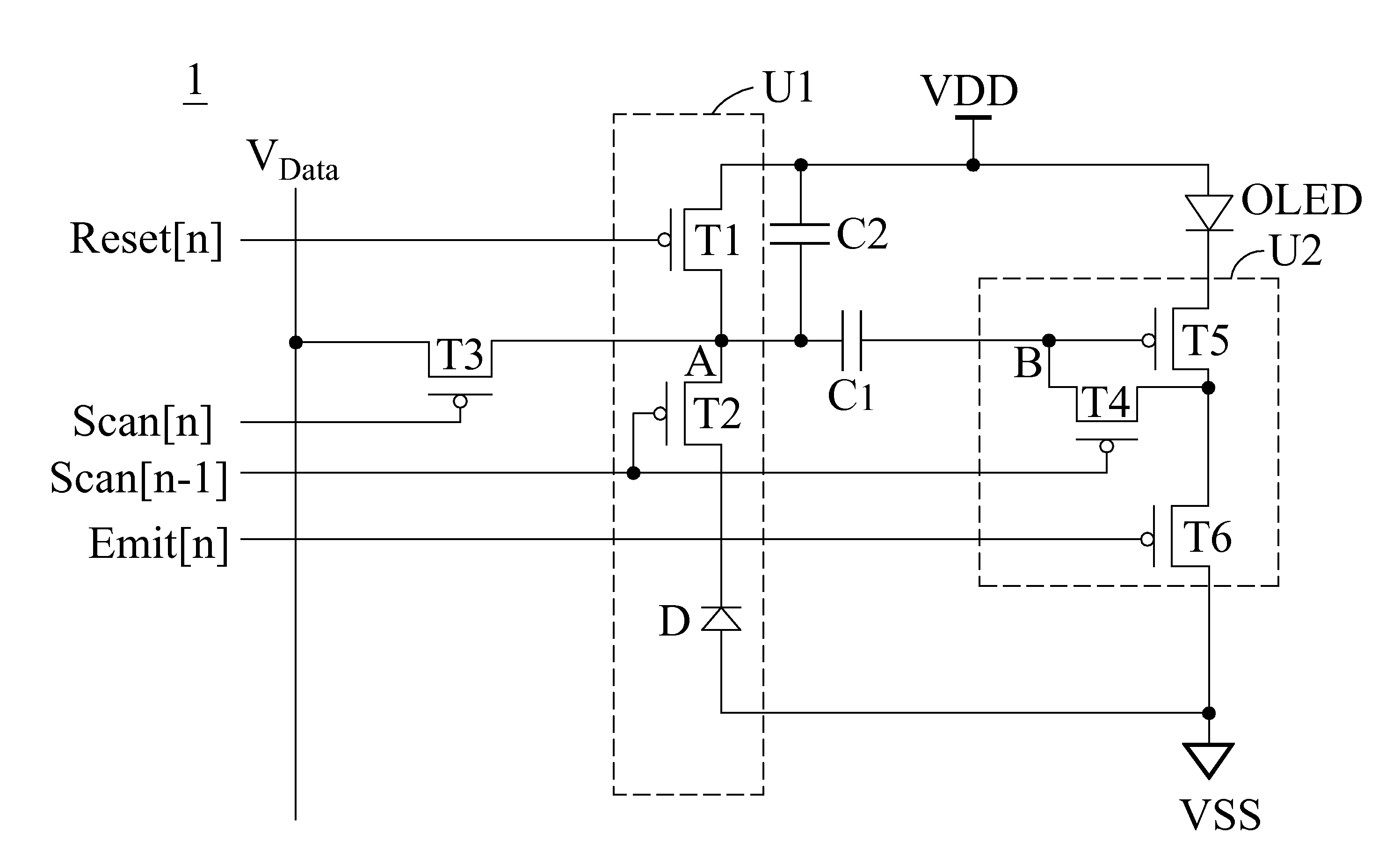
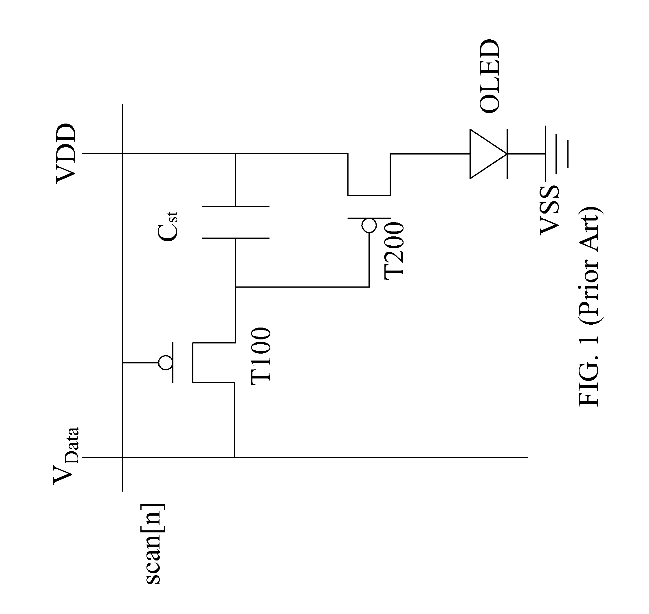
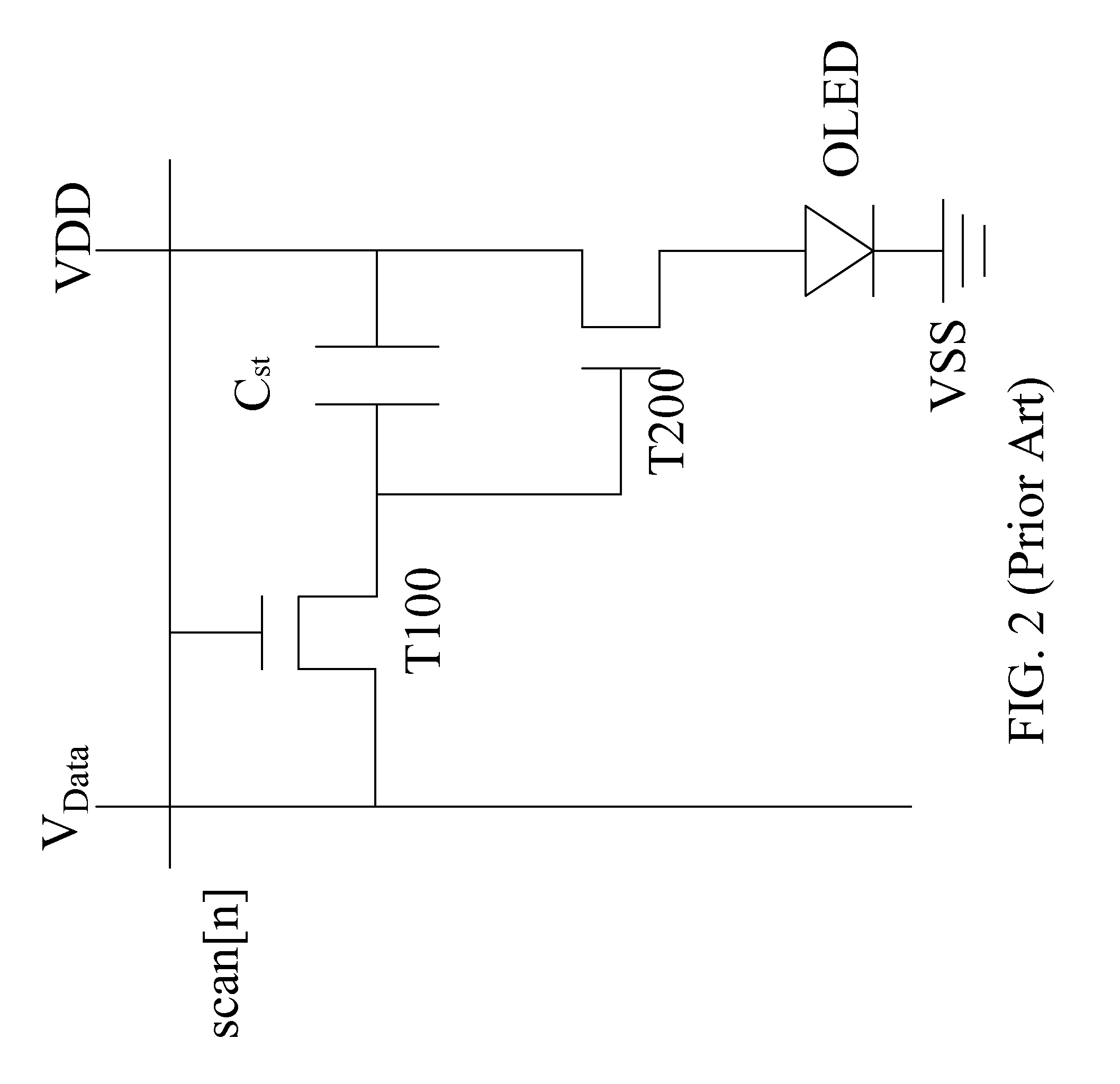
[0028]With reference to FIG. 4 for a schematic circuit diagram of a compensation circuit of an organic light emitting diode in accordance with the first preferred embodiment of the present invention, the compensation circuit of an organic light emitting diode 1 comprises seven P-type thin film transistors, a first capacitor C1, a second capacitor C2, a first control signal Reset[n], a second control signal Scan[n-1], a third control signal Scan[n], a fourth control signal Emit[n], a data voltage VData, a first power signal VDD, a second power signal VSS and an OLED. In the seven P-type thin film transistors, one serves as a photodiode, and the rest serve as a first P-type thin film transistor T1, a second P-type thin film transistor T2, a third P-type thin film transistor T3, a fourth P-type thin film transistor T4, a fifth P-type thin film transistor T5 and a sixth P-type thin film transistor T6 respectively. The first P-type thin film transistor T1, second P-type thin film transis...


PUM


Abstract

A compensation circuit of organic light emitting diode comprising a first capacitor, a second capacitor, a stabilizer unit, a third transistor, an organic light emitting diode and a driver unit. The stabilizer unit comprises a first transistor, a second transistor and a photodiode. The driver unit comprises a fourth transistor, a fifth transistor and a sixth transistor. The fifth transistor is used for driving the organic light emitting diode. The first transistor, the second transistor, the third transistor, the fourth transistor and the sixth transistor are used as switches. The first capacitor is used as a compensation capacitor. The second capacitor is used for storing a data voltage. By controlling a voltage of a node in the circuit, the current of the organic light emitting diode can be increased to maintain a stable brightness of the organic light emitting diode.

Description

CROSS-REFERENCE TO RELATED APPLICATION[0001]This application claims the benefit of priority to Taiwan Patent Application No. 100129312, filed on Aug. 16, 2011, in the Taiwan Intellectual Property Office, the disclosure of which is incorporated herein in its entirety by reference.BACKGROUND OF THE INVENTION[0002]1. Field of the Invention[0003]The present invention relates to a compensation circuit of an organic light emitting diode, in particular to the compensation circuit capable of maintaining a stable brightness of the organic light emitting diode.[0004]2. Description of the Related Art[0005]Active-matrix organic light-emitting diode (AMOLED) display device featuring thin thickness, light weight, self-luminescence, low driving voltage, high efficiency, high contrast, high color saturation, quick response speed, and high flexibility is considered as the most promising rising display technology after the development of thin film transistor liquid crystal display device (TFT-LCD).[0...

Claims


Application Information

Patent Timeline
Patent Type & Authority Applications(United States)
IPC IPC(8): H05B37/02
CPCG09G3/3233G09G2300/0819G09G2300/0861G09G2300/0852
Inventor KO, CHIEN-CHUANWU, CHAO-HUI
Owner HANNSTAR DISPLAY CORPORATION
Why Eureka
Try Eureka