Solar Metrology Methods And Apparatus

a metrology and solar energy technology, applied in the field of components inspection, can solve the problems of large surface defect density, low throughput capability, and inability to distinguish recombination events in the bulk of semiconductor materials, etc., to achieve the effect of improving yield and lowering manufacturing costs

Inactive Publication Date: 2013-02-28
KLA CORP
View PDF1 Cites 19 Cited by
  • Summary
  • Abstract
  • Description
  • Claims
  • Application Information

AI Technical Summary

Benefits of technology

[0008]Methods and apparatus for characterizing semiconductor wafers for solar cell manufacturing are presented. Specifically methods and apparatus to measure the photoluminescence of incoming wafers and extract parameters such as minority carrier life time, diffusion length, and defect density that can be used to predict final cell efficiency. Such measurements allow manufacturers to optimize manufacturing process based on incoming wafer quality to improve yield and lower manufacturing cost.
[0016]In yet another aspect, the surface of the wafer is passivated temporarily while undergoing inspection by any of the methods described herein. By passivating the surface of the wafer, electron-hole recombination at the surface can be reduced, allowing photons emitted from electron-hole recombination in the bulk of the wafer to be more visible in the light emitted at the wafer surface.

Problems solved by technology

However, wafers entering the solar manufacturing process (i.e., “as-cut” wafers) have a large density of surface defects (i.e., dangling bonds) that dominate the electron-hole recombination process.
These measurement techniques are unable to distinguish recombination events in the bulk of the semiconductor material from the relatively large number of recombination events at the surface.
In addition, photo-conductivity measurements have traditionally suffered from relatively low resolution and throughput capability.
Existing photoluminescence methods can generate high resolution full wafer images, but extracting relevant parameters demonstrating good correlation to final cell efficiency is difficult for similar reasons.

Method used


Image

  • Solar Metrology Methods And Apparatus
  • Solar Metrology Methods And Apparatus
  • Solar Metrology Methods And Apparatus

Examples


Embodiment Construction

[0047]Reference will now be made in detail to background examples and some embodiments of the invention, examples of which are illustrated in the accompanying drawings.

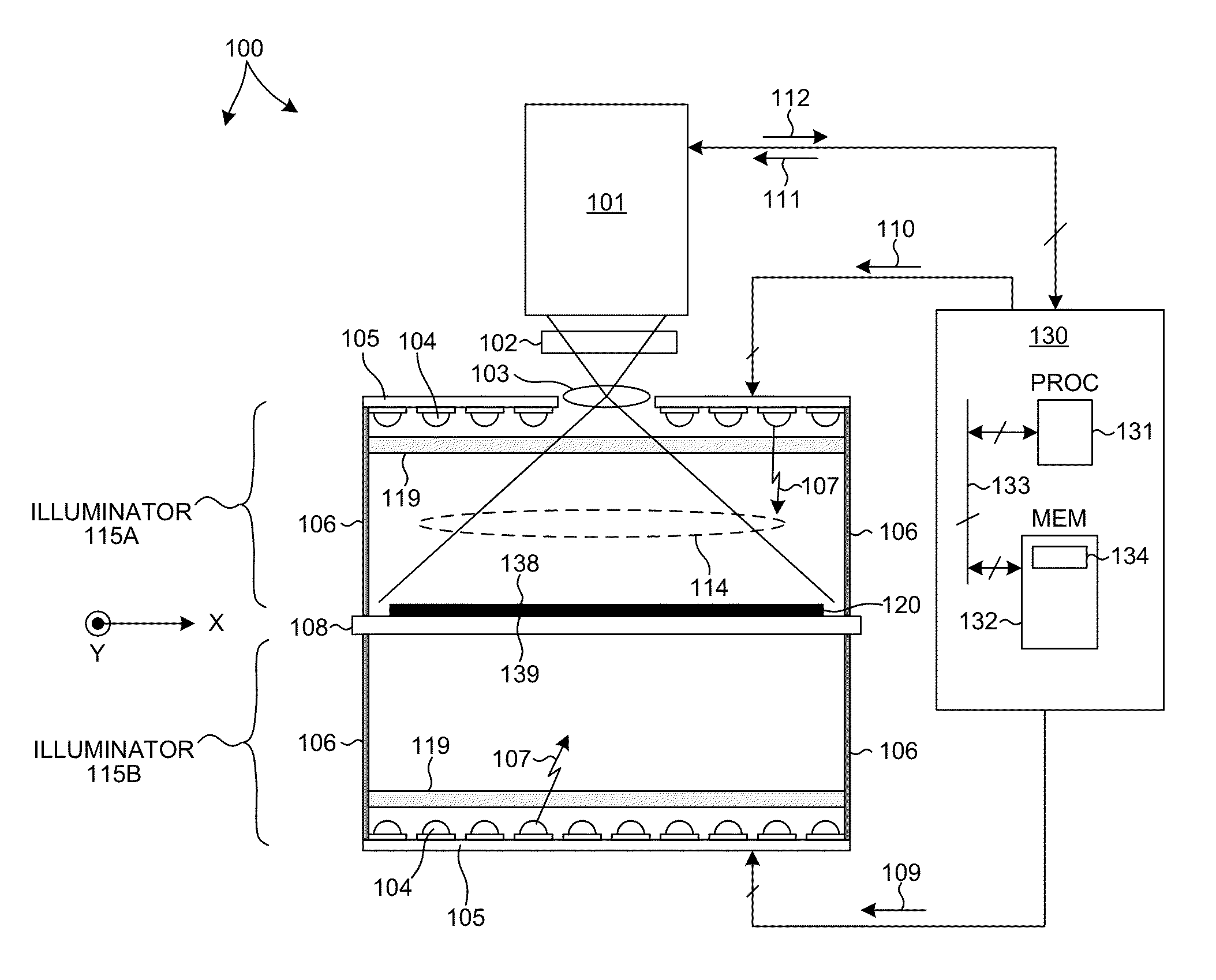
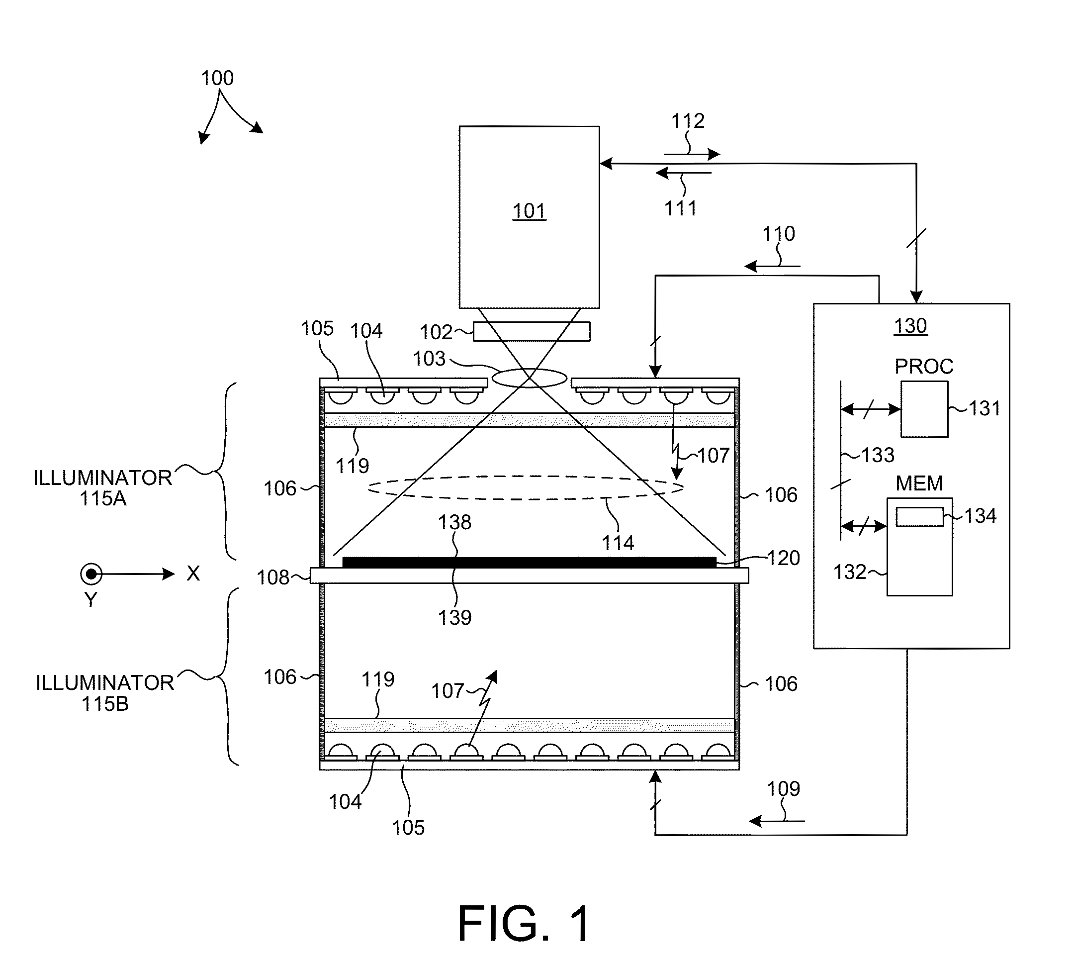
[0048]FIG. 1 is a simplified schematic view of one embodiment of an inspection system 100 that may be used to perform the inspection methods described herein. For simplification, some optical components of the system have been omitted. By way of example, folding mirrors, beam forming optics, polarizers, additional light sources, additional spectral filters, and additional light capture devices may also be included. All such variations are within the scope of the invention described herein. The inspection system described herein may be used for inspecting solar films, as well as semiconductor wafers.

[0049]As illustrated in FIG. 1, inspection system 100 includes a light capture device 101, a controller 130, a top side illuminator 115A and a bottom side illuminator 115B, and a specimen 120 under inspection. Each illumina...


PUM

PropertyMeasurementUnit
peak wavelengthaaaaaaaaaa

Abstract

Methods and apparatus are presented to measure the photoluminescence of incoming wafers and extract parameters such as minority carrier life time, diffusion length, and defect density that may be used to predict final solar cell efficiency. In some examples, illumination light is supplied to a side of an as-cut silicon wafer and the induced luminescence measured from the same side and the opposite side of the wafer is used to determine an indication of the minority carrier lifetime. In another example, the luminescence induced by two instances of illumination light of different wavelength is used to determine an indication of the minority carrier lifetime. In another example, the spatial distribution of luminescence intensity over an area surrounding a focused illumination spot is used to determine an indication of the minority carrier lifetime. Other apparatus useful to passivate the surface of a wafer for inspection are also presented.

Description

CROSS REFERENCE TO RELATED APPLICATION[0001]The present application for patent claims priority under 35 U.S.C. §119 from U.S. provisional patent application Ser. No. 61 / 512,309, entitled “Solar Metrology Methods and Apparatus,” filed Jul. 27, 2011, the subject matter of which is incorporated herein by reference.TECHNICAL FIELD[0002]The described embodiments relate to inspection of components used in the manufacture of solar power generating devices, and more particularly to estimation of bulk carrier lifetime.BACKGROUND INFORMATION[0003]Semiconductor materials are a fundamental building block of many solar power generating devices. The quality of the semiconductor structures that comprise these devices is critical to their overall power generating efficiency. Minority carrier life time and the related minority carrier diffusion length within a semiconductor structure are parameters used to characterize the quality of a semiconductor material and predict solar cell efficiency.[0004]T...

Claims


Application Information

Patent Timeline
Patent Type & Authority Applications(United States)
IPC IPC(8): G01N21/64
CPCH02S50/10G01N21/9501G01N21/6489Y02E10/50
Inventor YOUNG, SCOTTZHAO, GUOHENGLEVY, ADYGUEVREMONT, MARCOKHANNA, NEERAJ
Owner KLA CORP
Why Eureka
Try Eureka