
High Performance Power Transistor Having Ultra-Thin Package

Active Publication Date: 2013-02-28
TEXAS INSTR INC
View PDF4 Cites 6 Cited by
  • Summary
  • Abstract
  • Description
  • Claims
  • Application Information

AI Technical Summary

Benefits of technology

The patent describes a new power converters package that offers improved performance and reduced thickness. By cooling the transistor package from both surfaces and reducing the conduction and inductance losses, the package can handle higher currents and achieve higher efficiency and velocity. The package is designed with a reduced thickness pad for attachment of the chip and clips without bent rims to reduce parasitic resistance and inductance. The new assembly also allows for increased current handling and reduces the time it takes to turn the transistor on and off. The leadframe pad is designed with a rim to facilitate assembly. The fabrication process involves selecting a leadframe, etching a portion of the leadframe to reduce its thickness, attaching the FET chip to the pad with conductive adhesive or solder, connecting the source and gate of the FET to package terminals with clips, and reducing parasitic resistances and inductance by using clips without bent rims.

Problems solved by technology

These wires may introduce, due to their lengths and resistances, significant parasitic inductance into the power circuit.
After this attachment, the leadframe pad is remote from the PCB, but since it is divided into two portions serving two die terminals, a heat sink cannot be attached to the pad.
This means, the leadframe cannot be stamped.

Method used


Image

  • High Performance Power Transistor Having Ultra-Thin Package
  • High Performance Power Transistor Having Ultra-Thin Package
  • High Performance Power Transistor Having Ultra-Thin Package

Examples


Embodiment Construction

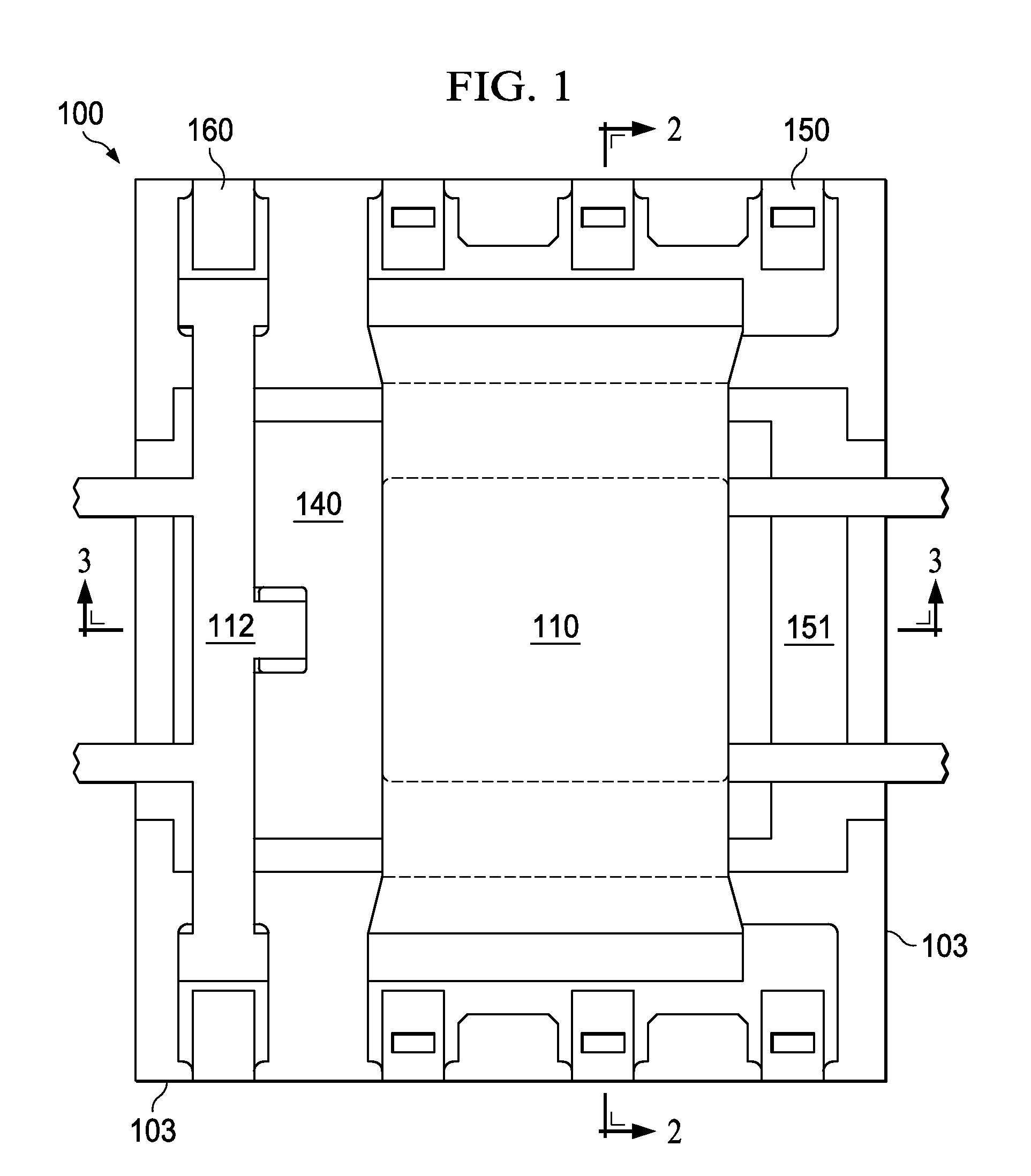
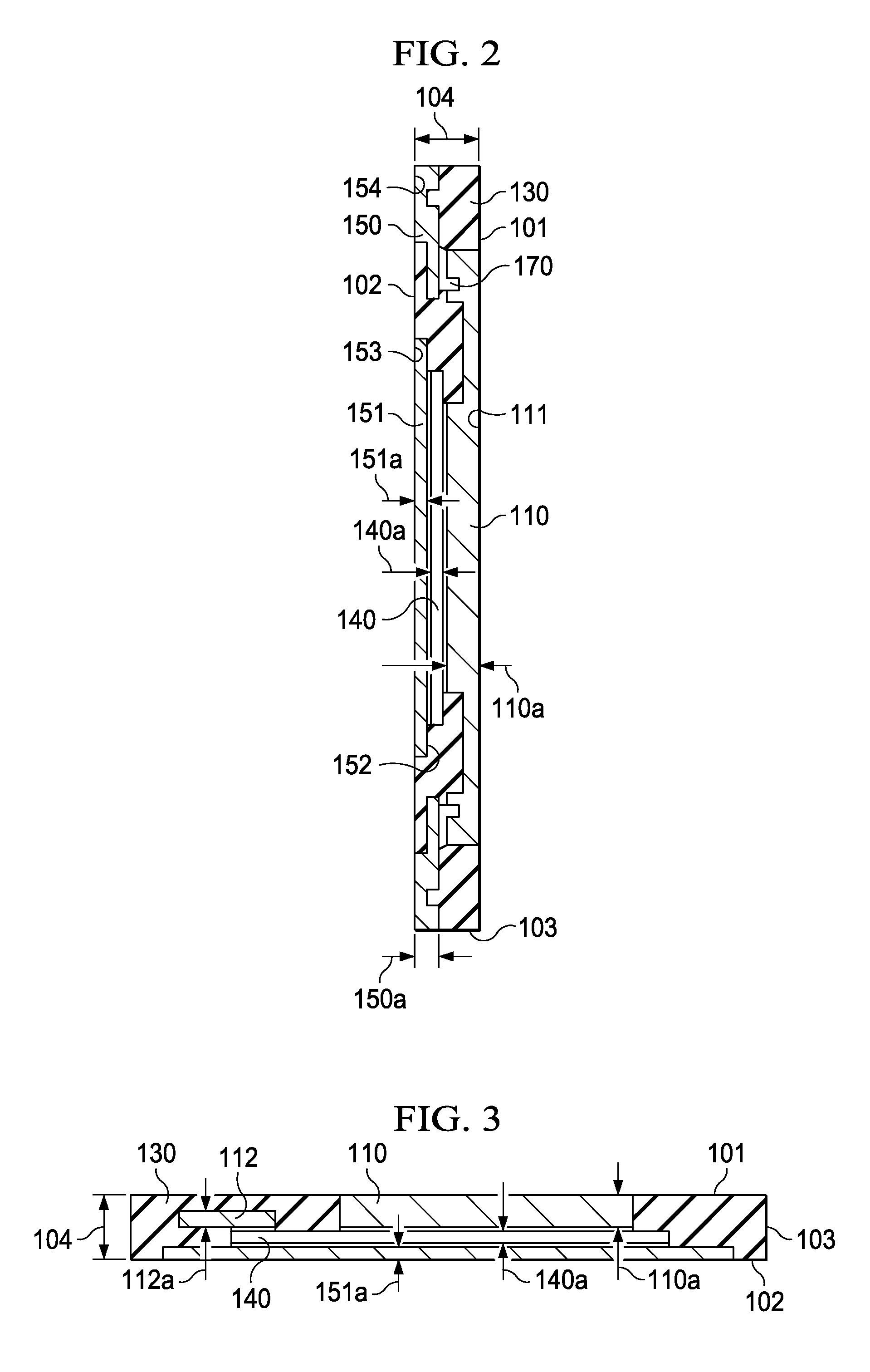
[0019]FIGS. 1, 2, and 3 illustrate an exemplary embodiment of the invention, the package of a semiconductor power chip 140 intended for assembly on a substrate such as a motherboard. The package is particularly useful for packaging power field effect transistors (FET), power switches, power converters, which handle large electrical currents (for example, 25 to 40 A) and thus generate significant heat. Chip 140 has a thickness 140a; for the example shown, thickness 140a is preferably about 0.05 mm; in other embodiments, chip 140 may be thicker or thinner. The FET has a first, a second and a third terminal. The power device, generally designated 100, is depicted in top view (FIG. 1) and in cross sections FIGS. 2 and 3). The cutaway lines in FIG. 1 indicate the positions of the cross sections. For clarity's sake, the top view of FIG. 1 is depicted under the assumption that the packaging compound 130 is transparent; in reality, the insulating compound has to be opaque (for instance a bl...


PUM


Abstract

A field-effect transistor package includes a leadframe with a first linear thickness (150a) and a leadframe pad (151) of a reduced thickness; a first terminal of a field-effect transistor chip (140) attached to the pad and a second and a third terminal remote from the pad; a metal sheet (110) of a second linear thickness (110a) connecting the second transistor terminal to a package terminal; a metal sheet (112) of a third linear thickness (112a) connecting the third transistor terminal to a package terminal; the sum of the first linear thickness (about 0.125 mm) and the second linear thickness (about 0.125 mm) plus attach material (about 0.05 mm) comprising the package thickness (about 0.3 mm).

Description

FIELD OF THE INVENTION[0001]The present invention is related in general to the field of semiconductor devices and processes, and more specifically to the structure and fabrication method of ultra-thin QFN-packaged power transistors capable of high current, high efficiency, and high velocity.DESCRIPTION OF RELATED ART[0002]For many of today's power switching devices, the chips of the power MOSFETs are assembled as individual components. The devices use a metallic leadframe, which typically has a rectangular pad surrounded by leads; the pad serves as substrate for attaching the semiconductor chip and the leads serve as output terminals. The leads are commonly shaped without cantilever extensions, and arranged in the manner of Quad Flat No-Lead (QFN) or Small Outline No-Lead (SON) devices. The electrical connections from the chip to the leads can be provided in several ways.[0003]In one family of devices, the connections are provided by bonding wires. These wires may introduce, due to ...

Claims


Application Information

Patent Timeline
IPC IPC(8): H01L29/78H01L23/495
CPCH01L23/3107H01L23/49503H01L23/49524H01L23/49562H01L2924/1306H01L2924/13091H01L24/34H01L2224/32245H01L2924/00H01L2924/181H01L2224/40245H01L24/40H01L2224/371H01L24/37H01L2224/37147H01L2224/37599H01L2224/3716H01L2224/8385H01L2224/83801H01L2224/84801H01L2224/8485H01L24/84H01L24/41H01L2224/4103H01L2224/32257H01L2224/37124H01L2224/73263H01L2924/00012H01L2924/0781H01L2924/00014H01L24/36
Inventor HERBSOMMER, JUAN A.LOPEZ, OSVALDO J.NOQUIL, JONATHAN A.
Owner TEXAS INSTR INC
Learn More