
Programmable non-volatile memory

a non-volatile memory and programmable technology, applied in solid-state devices, diodes, instruments, etc., can solve the problems of the need of access transistors, the fundamental limitation of increasing the integration density, and the need of thick oxide layer mos transistors, so as to increase the integration density and facilitate the fabrication process. , the effect of improving the integration density

Active Publication Date: 2013-02-28
RANGDURU
View PDF7 Cites 36 Cited by
  • Summary
  • Abstract
  • Description
  • Claims
  • Application Information

AI Technical Summary

Benefits of technology

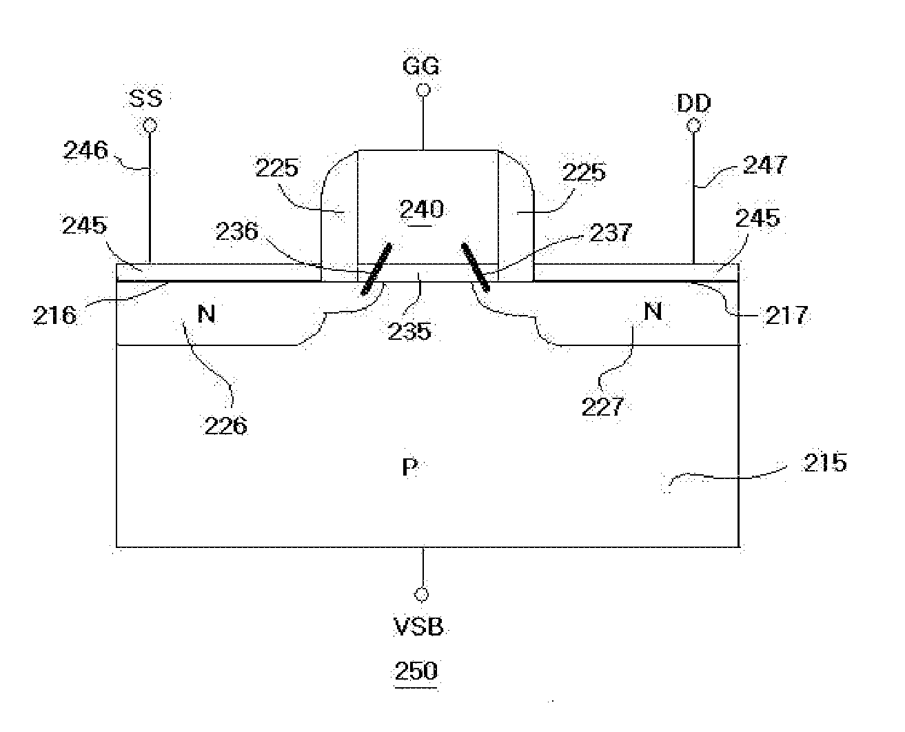
The present invention provides a memory cell and operation method that increases the integration density compared to previous designs. It utilizes a single transistor and two diodes, which allows for a more efficient use of space. The fabrication process is easier and area-efficient, as it only requires a single thin oxide layer thickness compared to prior art designs that require two oxide layer thicknesses. Overall, the present invention provides a more efficient and easier to fabricate two-bit storable memory cell.

Problems solved by technology

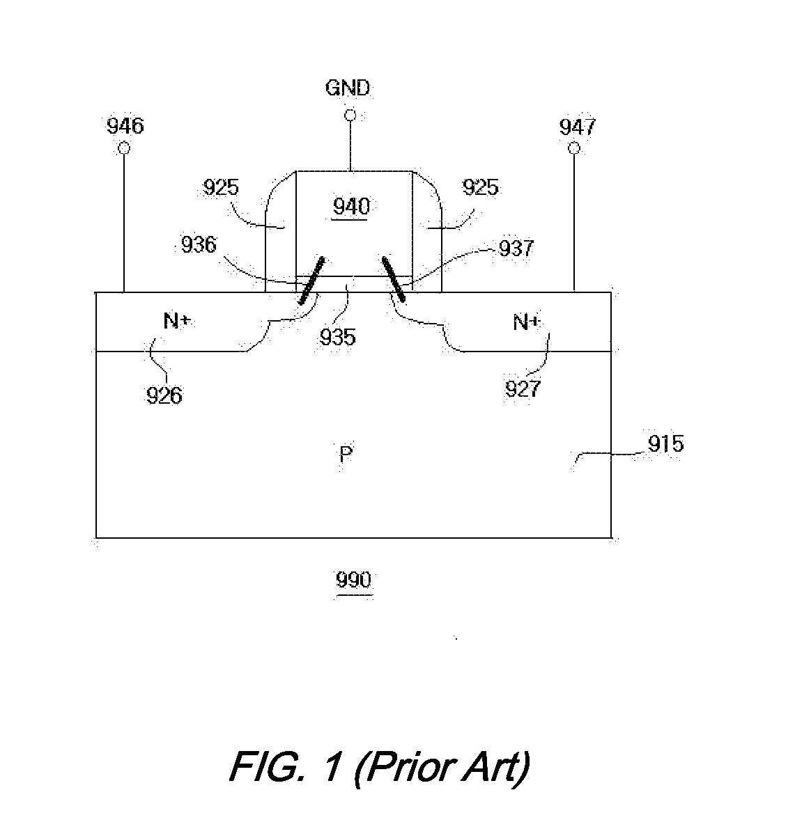
It is a disadvantage that a thick oxide layer MOS transistor is needed in the access MOS transistor to be suitable for high voltage operation while a thin oxide layer MOS transistor is used in the storage MOS transistor 990.
It is also a disadvantage that the need of the access transistor is the fundamental limitation in increase of the integration density.
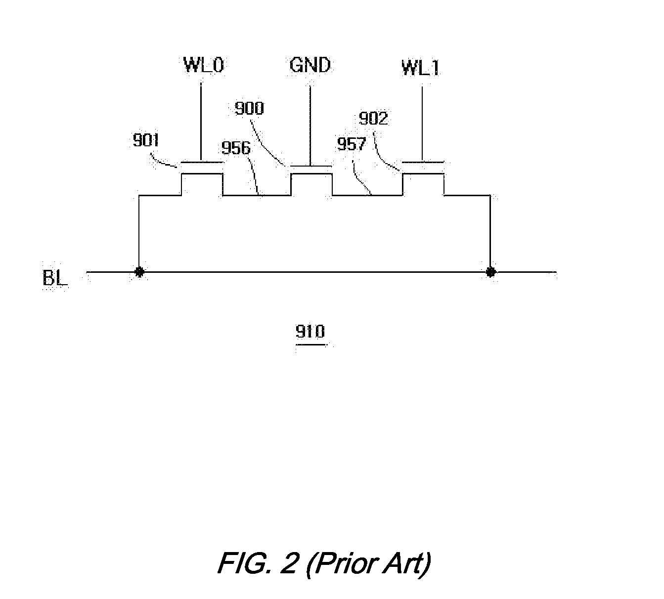
As described previously, the device includes the access transistors and it is the fundamental limitation in increase of the integration density.
According to the prior art, the fabrication process becomes relatively complicated because the memory cell should be fabricated in high density MOS transistors with two different oxide layer thicknesses.
Further, three transistors are required to make a two-bit storable memory cell, being the fundamental limitation in increase of the integration density.

Method used


Image

  • Programmable non-volatile memory
  • Programmable non-volatile memory
  • Programmable non-volatile memory

Examples


Embodiment Construction

[0056]An aspect or aspects of present invention will now be described more fully with reference to the accompanying drawings, in which exemplary embodiments of the invention are shown.

[0057]The embodiments of the present invention are provided to fully describe the present inventive concept to those of ordinary skill in the art, may be embodied in many different forms, and should not be construed as being limited to the embodiments set forth herein; rather, these embodiments are provided so that this disclosure will be thorough and complete, and will fully convey the concept of the present inventive concept.

[0058]The terminology used in the application is used only to describe specific embodiments and does not have any intention to limit the inventive concept. An expression in the singular includes an expression in the plural unless they are clearly different from each other in a context. In the application, it should be understood that terms, such as “comprise” and / or “comprising”,...


PUM


Abstract

A programmable non-volatile memory including a memory cell includes a transistor acting as an anti-fuse and two diodes for access. The memory cell that can store two bits and includes a transistor acting as an anti-fuse and two diodes for access, wherein the cell transistor includes: the source electrode formed by a metal; the first diode as the source region contact structure; the drain electrode formed by a metal; and the second diode as the drain region contact structure wherein the cell transistor, the oxide layer between the source area and the gate is the first anti-fuse the first storage; the oxide layer between the drain area and the gate is the second anti-fuse the second storage; the two diodes are connected in series to access the two anti-fuses.

Description

CROSS-REFERENCE TO RELATED APPLICATIONS[0001]This application claims the benefit of Korean Patent Application No. 10-2011-0085734, filed on Aug. 26, 2011, in the Korean Intellectual Property Office, the disclosure of which is incorporated herein in its entirety by reference.BACKGROUND[0002]1. Filed[0003]One or more embodiments relate to a one-time-programmable non-volatile memory device, and more particularly relates to a programmable non-volatile memory device, including a transistor acting as an anti-fuse and two diodes for access.[0004]2. Related Art[0005]Korea Patent Publication 10-2001-0056831 relates to a method of making an anti-fuse of the semiconductor device, and more particularly relates to a method of making an anti-fuse of the semiconductor device using a right-angled corner of the semiconductor substrate to cause the breakdown of the insulator layer at a lower voltage, wherein the method of making an anti-fuse of the semiconductor device comprises: a step making right-...

Claims


Application Information

Patent Timeline
IPC IPC(8): H01L27/088G11C17/06
CPCG11C17/06H01L27/1021H01L27/101G11C17/18
Inventor KWON, EUIPIL
Owner RANGDURU
Learn More