Display device

Active Publication Date: 2013-03-14
JAPAN DISPLAY INC
View PDF3 Cites 15 Cited by
  • Summary
  • Abstract
  • Description
  • Claims
  • Application Information

AI Technical Summary

Benefits of technology

[0014]According to the present invention, the occurrence of the uneven brightnes

Problems solved by technology

This can cause a signal delay to occur even in the video signals output to the video signal lines and the scanning signals output to the scanning signal lines.
This mak

Method used


Image

  • Display device
  • Display device
  • Display device

Examples


first embodiment

(Overall Configuration)

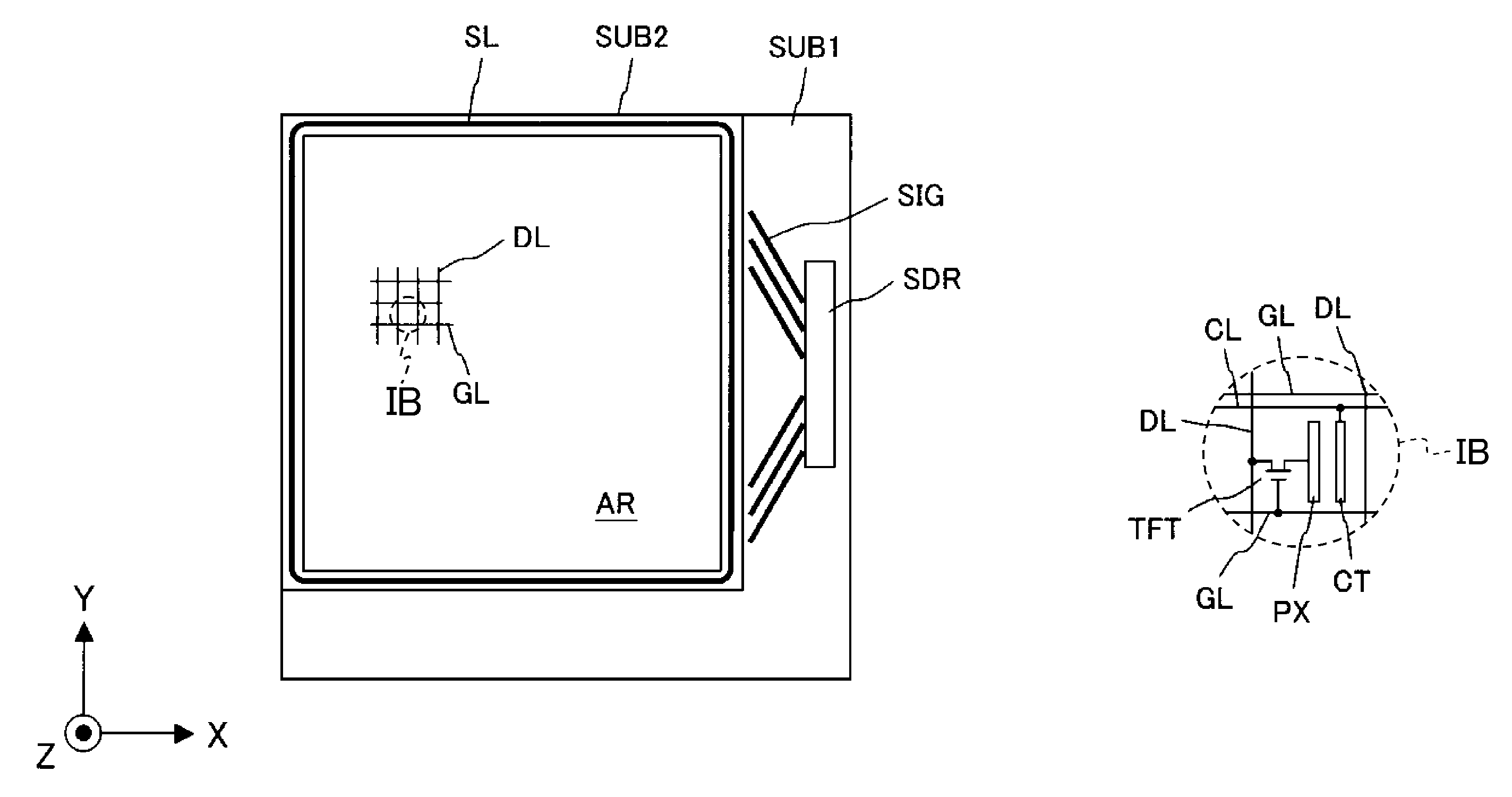
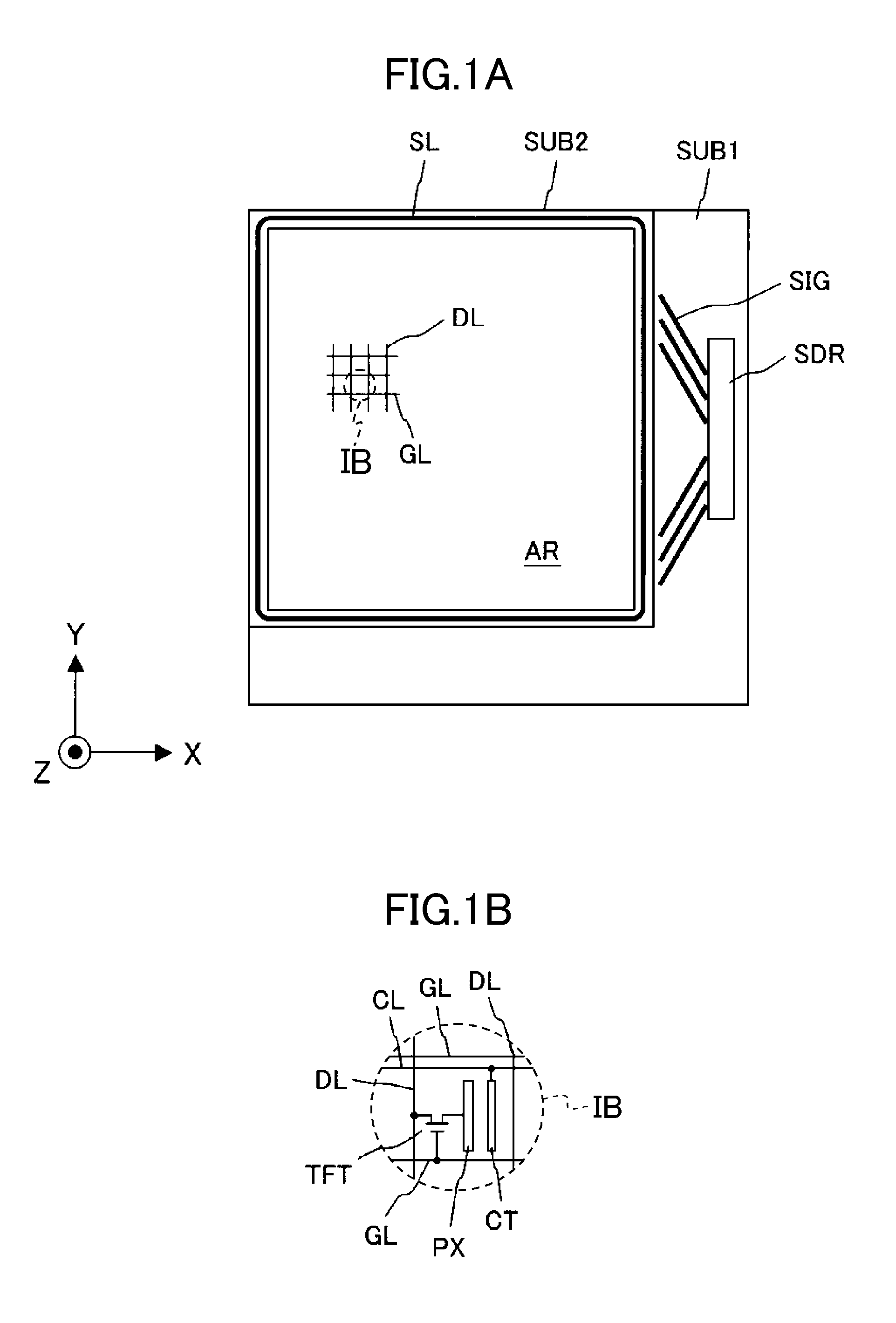
[0037]FIG. 1A is a diagram illustrating an outline configuration of a liquid crystal display device which is a display device according to a first embodiment of the present invention. Hereinafter, a description will be given of an overall configuration of a liquid crystal display device according to the first embodiment with reference to FIG. 1A. In the following description, the present invention is applied to the liquid crystal display device using a liquid crystal display panel of an IPS (in-plane switching) system. However, the present invention can be applied to a liquid crystal display panel of a TN (twisted nematic) system, a VA (vertical alignment) system or the like. Further, the display panel that conducts image display is not limited to a non-emissive type liquid crystal display panel, but can be also applied to another non-emissive type display panel, or an emissive type display panel such as an organic EL display panel or a plasma display panel. A...

second embodiment

[0062]FIG. 7 is an enlarged view of a peripheral portion in a liquid crystal display device which is a display device according to a second embodiment of the present invention, and FIG. 8 is a cross-sectional view taken along a line VIII-VIII illustrated in FIG. 7. In the liquid crystal display device according to the second embodiment, the other configurations except for the configuration of a conductive film MIT are identical with those in the first embodiment, and therefore, in the following description, the conductive film MIT will be described in detail.

[0063]As illustrated in FIG. 7, in the liquid crystal display device according to the second embodiment, the conductive film MIT different from the shield electrode CS is formed, the lead lines SIG2 each having the shorter wiring length of the lead lines SIG1 and SIG2 formed in the peripheral portion, and the conductive film MIT overlap with each other when viewed in a plane. In this case, the shield electrode CS has an extensio...

third embodiment

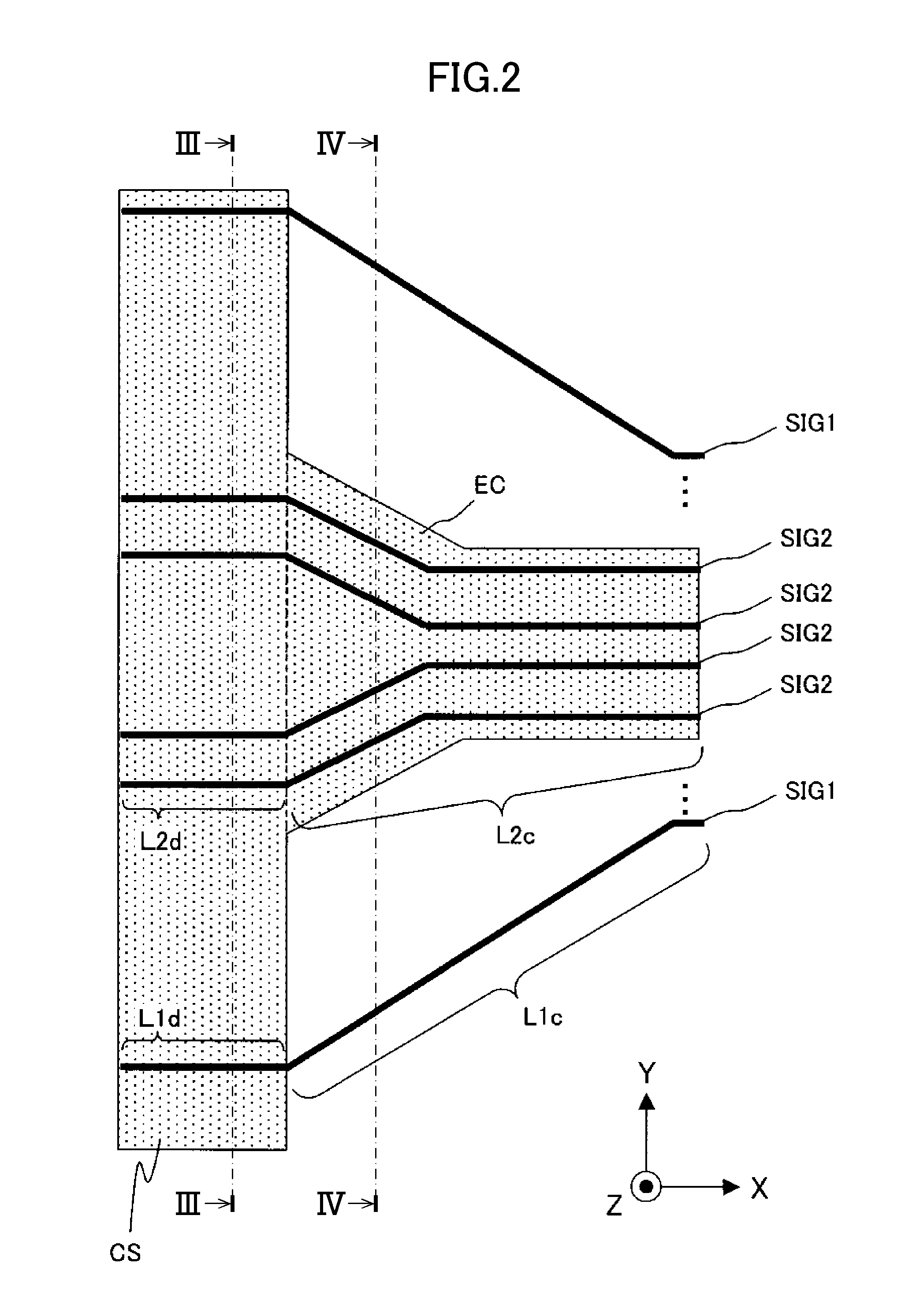
[0072]FIG. 10 is a diagram illustrating an outline configuration of lead lines in a liquid crystal display device which is a display device according to a third embodiment of the present invention. The other configurations except for the configuration of conductive films EC1 and EC2 superposed on the lead lines SIG1 and SIG2 are identical with those in the first embodiment.

[0073]As is apparent from FIG. 10, the conductive films EC1 and EC2 overlap with all of the lead lines SIG1 and SIG2. Further, in the conductive films EC1 and EC2 according to the third embodiment, the conductive film EC1 or EC2 is formed for each of the lead lines SIG1 and SIG2 along the extension direction thereof. The conductive films EC1 and EC2 that extend from the shield electrode CS are arrayed in parallel to the Y-direction. With the above configuration, in the conductive films EC1 and EC2 according to the third embodiment, the amount of superposition can correspond to the respective lead lines SIG, and th...


PUM


Abstract

A display device includes lead lines that extend from a display area, and electrically connect video signal lines or scanning signal lines within a display area, and a driver circuit or a terminal portion that receives an output from the driver circuit; an insulating film that is formed in an upper layer of the lead lines and covers the lead lines; and a conductive film that is formed in an upper layer of the insulating film. The lead lines include a plurality of first lead lines that start from the driver circuit or the terminal portion, and arrive at the scanning signal lines or the video signal lines, and a plurality of second lead lines that are smaller in wiring resistance than the first lead lines. At least the first lead lines overlap with the conductive film through the insulating film.

Description

CROSS-REFERENCE TO RELATED APPLICATION[0001]The present application claims priority from Japanese application JP2011-198130 filed on Sep. 12, 2011, the content of which is hereby incorporated by reference into this application.BACKGROUND OF THE INVENTION[0002]1. Field of the Invention[0003]The present invention relates to a display device, and more particularly to a lead line formed on a peripheral portion of a display area.[0004]2. Description of the Related Art[0005]In a related-art liquid crystal display device, a plurality of video signal lines that supply a video signal, and a plurality of scanning signal lines that are so formed as to intersect with the video signal lines to supply a scanning signal are formed on a liquid crystal surface side of one transparent substrate of a pair of transparent substrates which are opposed to each other through a liquid crystal, layer. A plurality of pixels are formed respectively in an area surrounded by the video signal lines and the scanni...

Claims


Application Information

Patent Timeline
IPC IPC(8): G09G3/36G06F3/038
CPCG02F1/1345G02F1/13452G02F1/136286G02F1/1343G02F1/1368
Inventor NISHINO, TOMONORIYANAGISAWA, SYOUSAITOU, MASANARIAOKI, YOSHINORIISHIGE, NOBUYUKI
Owner JAPAN DISPLAY INC
Why Eureka
Try Eureka