EL display panel, EL display apparatus, and method of manufacturing EL display panel

a technology of thin film semiconductors and display panels, which is applied in the manufacture of electrode systems, electric discharge tubes/lamps, and discharge tubes luminescnet screens, etc., can solve the problems of increasing parasitic capacitance between the gate line and the power supply line, unsatisfactory reduction of the resistance of the gate line, and uneven brightness of the light emitted from the display apparatus. , to achieve the effect of small heat conductivity and small heat conductivity increase the resistivity of the material

Active Publication Date: 2012-09-25
JOLED INC
View PDF29 Cites 8 Cited by
  • Summary
  • Abstract
  • Description
  • Claims
  • Application Information

AI Technical Summary

Benefits of technology

[0019]However, in the thin film semiconductor device for display apparatus disclosed in Patent Literature 2, the integrated portion of the gate electrode and the gate line are still made of the same material. Accordingly, forming the gate electrode with the material having small heat conductivity increases the resistivity of the material composing the integrated portion of the gate line, increasing the resistance of the integrated portion of the gate line. As a result, there is a problem that the line resistance of the gate line is not sufficiently reduced, causing uneven brightness of light emitted from the display apparatus.
[0024]The present invention has been conceived to solve the problems above, and it is an object of the present invention to provide an EL display panel which is capable of preventing uneven brightness in the emitted light and extending the product life, and in which the region for arranging thin film transistors is not limited by the space for lines.
[0026]According to the EL display panel of the present invention, the gate lines and the gate electrodes can be formed in different layers. Thus, it is possible to select materials suitable for the gate lines and gate electrodes separately to reduce the line resistance and improve the brightness of the light emitted from the EL display panel.
[0027]In addition, the power supply line as the TFT power supply line is formed in the same layer as the gate lines, and thus it is possible to reduce parasitic capacitance between the power supply line and the gate line. Furthermore, since the auxiliary line as the EL power supply line is formed in the same layer as the gate line, it is not necessary to form a separate auxiliary line in the EL unit. This increases the aperture ratio of the pixels, thereby increasing the life of the display panel.
[0028]Furthermore, since the power supply line and the auxiliary line are formed in the same layer as the gate line and side-by-side with the gate line. Thus, it is possible to reduce the unevenness caused by the gate line on the interlayer insulating film by the power supply line and the auxiliary line. With this, it is possible to improve the flatness, and increase the life of the EL display panel.
[0029]Furthermore, the power supply lines shared by pixels are provided, thereby reducing the space for arranging the power supply line which used to be provided for each pixel. Therefore, it is possible to provide an EL display panel in which the space for arranging the thin film transistors is not limited by the space for the lines.FURTHER INFORMATION ABOUT TECHNICAL BACKGROUND TO THIS APPLICATION

Problems solved by technology

As a result, there is a problem that the line resistance of the gate line is not sufficiently reduced, causing uneven brightness of light emitted from the display apparatus.
Thus, there is a problem that even one bad connection in the connected portion of the integrated portion and the separate portion results in disconnection of all of the pixels in one line along the gate line.
Thus, in an area where the gate line and the power supply line cross each other, the interval between the gate line and the power supply line is narrow, which increases parasitic capacitance between the gate line and the power supply line.
This parasitic capacitance may cause unevenness in the brightness of light emitted from the display apparatus.
In addition, there is a limit in an attempt to increase the thickness of the gate insulating film to reduce the parasitic capacitance.
The limit is set to secure the capability of the thin film semiconductor device, and the thickness of the gate insulating film cannot be increased beyond the limit.
There is a problem that the EL power supply line reduces the aperture ratio of the panel of the display apparatus, and consequently, the life of the EL display apparatus is not sufficient.

Method used


Image

  • EL display panel, EL display apparatus, and method of manufacturing EL display panel
  • EL display panel, EL display apparatus, and method of manufacturing EL display panel
  • EL display panel, EL display apparatus, and method of manufacturing EL display panel

Examples


first embodiment

[0112](First Embodiment)

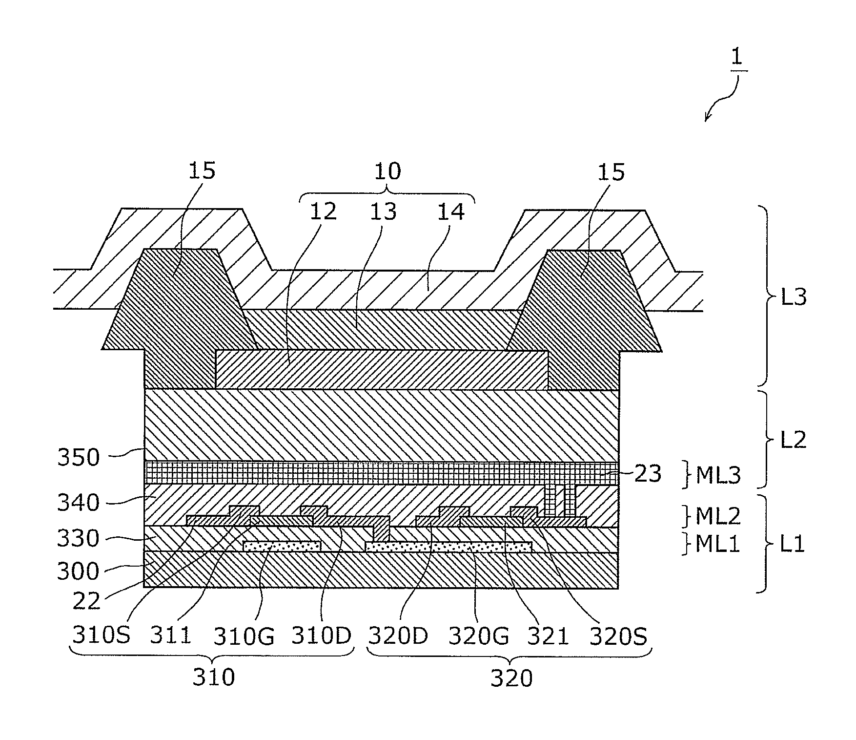
[0113]First, the organic electro-luminescence (EL) panel according to the first embodiment of the present invention shall be described with reference to FIG. 1. FIG. 1 is a partial cutout perspective view of an organic EL display panel according to the first embodiment of the present invention.

[0114]As illustrated in FIG. 1, the EL display panel 1 according to the first embodiment of the present invention is an organic EL display panel (organic EL display), and includes an organic EL device 10 which is a light-emitting display device, and a thin film semiconductor array device 20 composed of an active matrix substrate in which a thin film transistor and lines are formed. Note that, the organic EL device 10 corresponds to the EL unit according to the present invention, and the thin film semiconductor array device for display apparatus 20 corresponds to the thin film semiconductor unit in the present invention.

[0115]The organic EL device 10 includes a lower ele...

second embodiment

[0228](Second Embodiment)

[0229]The following describes the circuit configuration of the pixel in the EL display panel according to the second embodiment of the present invention with reference to FIGS. 19 to 21. FIG. 19 is a planar view of the thin film semiconductor device for display apparatus provided in the EL display panel according to the second embodiment of the present invention. FIG. 20 is a cross sectional view of the thin film semiconductor device for display apparatus along X2-X2′ in FIG. 19. FIG. 21 is a diagram for describing TFT characteristics of thin film transistors in the thin film semiconductor device for display apparatus according to the first embodiment of the present invention.

[0230]The thin film semiconductor device for display apparatus 3 in the EL display panel according to the second embodiment of the present invention has the same basic configuration as the thin film semiconductor device for display apparatus 2 in the EL display panel according to the fi...


PUM


Abstract

An EL display panel including an EL unit and a thin film semiconductor unit, in which the EL unit includes an anode electrode, a cathode electrode, and a light-emitting layer, and the thin film semiconductor unit includes a substrate, a gate electrode, a gate insulating film, a semiconductor layer, a first electrode, a second electrode, an interlayer insulating film, a gate line formed above the interlayer insulating film, a power supply line formed above the interlayer insulating film, in a same layer as the gate line, and side-by-side with the gate line, and an auxiliary line formed above the interlayer insulating film, in a same layer as the gate line and the power supply line, and side-by-side with the gate line and the power supply line.

Description

CROSS REFERENCE TO RELATED APPLICATION[0001]This is a continuation application of PCT application No. PCT / JP2010 / 005846 filed on Sep. 29, 2010, designating the United States of America.BACKGROUND OF THE INVENTION[0002](1) Field of the Invention[0003]The present invention relates to thin film semiconductor devices and EL display panels using the thin film semiconductor devices and methods of manufacturing EL display apparatuses and EL display panels, and particularly relates to a thin film semiconductor device used for an active-matrix display apparatus and a method of manufacturing the same.[0004](2) Description of the Related Art[0005]Thin film transistors (TFT) are used as a switching device for selecting pixel or a driving device for display device in active-matrix drive display apparatuses such as liquid crystal display apparatuses and organic EL display apparatuses.[0006]TFTs are used for active-matrix substrate of display apparatuses, and active research and development have b...

Claims


Application Information

Patent Timeline
Patent Type & Authority Patents(United States)
IPC IPC(8): H05B33/00
CPCH01L27/3276H10K59/131H10K10/46H10K50/824
Inventor KANEGAE, ARINOBU
Owner JOLED INC
Why Eureka
Try Eureka