Liquid Crystal Display Device and Method for Manufacturing the Same

a technology of liquid crystal display and manufacturing method, which is applied in the manufacture of electrode systems, electric discharge tubes/lamps, instruments, etc., can solve the problems of inability to smoothly perform image cannot normally be displayed, and the test of a manufactured panel cannot be smoothly performed, so as to increase the manufacturing efficiency and prevent the effect of disconnection

Active Publication Date: 2013-03-28
LG DISPLAY CO LTD
View PDF4 Cites 79 Cited by
  • Summary
  • Abstract
  • Description
  • Claims
  • Application Information

AI Technical Summary

Benefits of technology

[0055]An aspect of the present invention is directed to provide an LCD device and a method of manufacturing the same, which a passivation layer and a pixel electrode are simultaneously formed by a single mask process using a half tone mask, and thus, manufacturing efficiency increases.
[0056]Another aspect of the present invention is directed to provide an LCD device and a method of manufacturing the same, which can prevent disconnection, caused by loss of a pixel electrode due to a lift-off process, in a pad area.
[0057]Another aspect of the present invention is directed to provide an LCD device and a method of manufacturing the same, which can the contact performance of a pixel bar in a pad area.

Problems solved by technology

In this way, if the pixel electrode 90 is lost in the pad area, respective signals cannot be supplied to a plurality of pixels formed in the active area, and thus, the test of a manufactured panel is not smoothly performed, and moreover defective driving occurs in which an image cannot normally be displayed.
For this reason, the test of a manufactured panel cannot smoothly be performed.
Also, defective driving occurs in which an image cannot normally be displayed.
In this way, in manufacturing the related art LCD device with integrated touch sensor, a number of masks are used, and thus, the manufacturing cost increases.
Moreover, since a detailed process is performed in each mask process, the manufacturing cost is high, and a time taken in manufacturing is long, causing the decrease in product competitiveness.

Method used


Image

  • Liquid Crystal Display Device and Method for Manufacturing the Same
  • Liquid Crystal Display Device and Method for Manufacturing the Same
  • Liquid Crystal Display Device and Method for Manufacturing the Same

Examples


first embodiment

[0094]FIG. 7 is a view illustrating an LCD device according to an embodiment of the present invention. FIG. 8 is a view illustrating a pixel structure of an LCD device according to the present invention;

[0095]In FIGS. 7 and 8, the structure of a thin film transistor (TFT) array substrate (lower substrate) is illustrated in the FFS mode. In FIGS. 7 and 8, a touch sensor is illustrated as being internalized in an in-cell touch type in the TFT array substrate.

[0096]In FIGS. 7 and 8, a color filter array substrate (upper substrate), a liquid crystal layer, a backlight unit, and a driving circuit part are not illustrated.

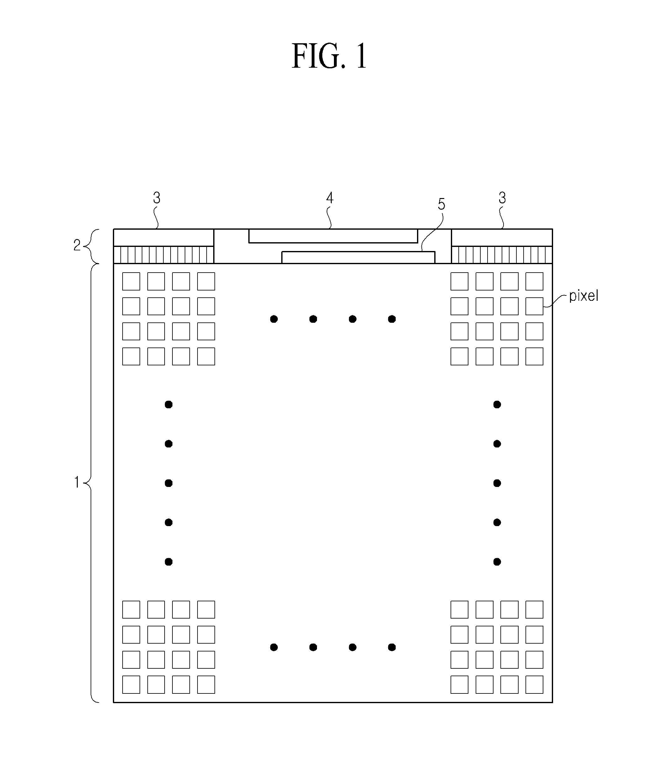
[0097]Referring to FIG. 7, an active area 100 displaying an image is formed at a TFT array substrate, and an inactive area is formed at an outer portion of the active area 100. A plurality of pixels are formed in the active area 100. Furthermore, a plurality of pad parts 230, 240 and 250 are formed in the inactive area 200.

[0098]The plurality of pad parts 230, 240 and 25...

second embodiment

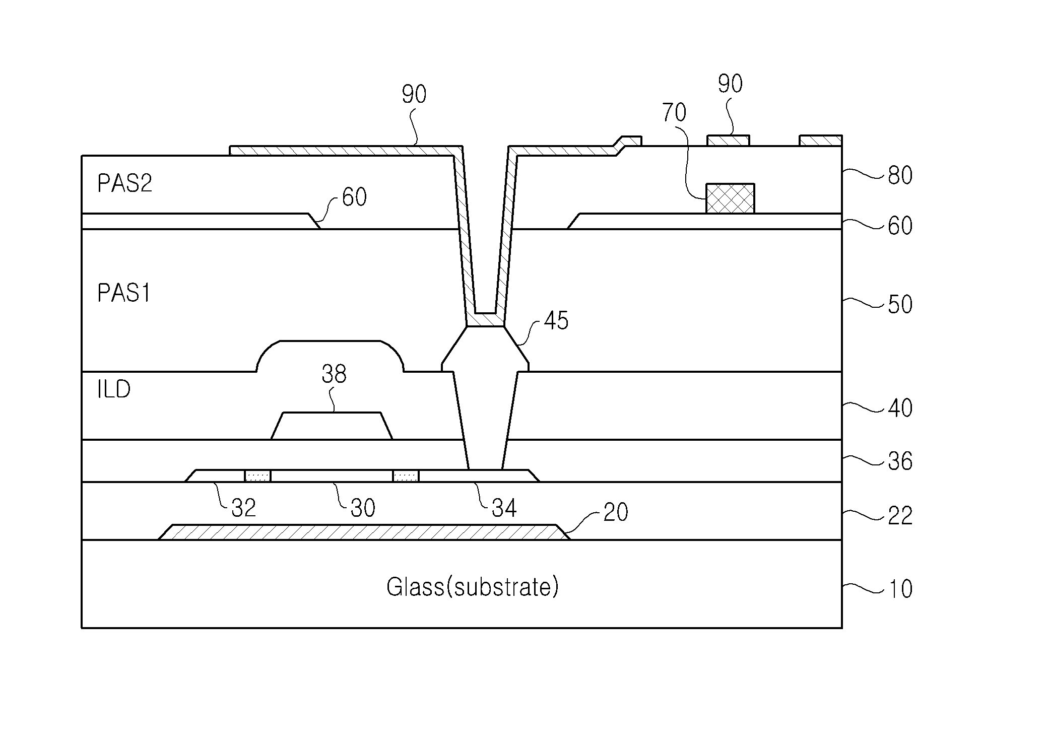
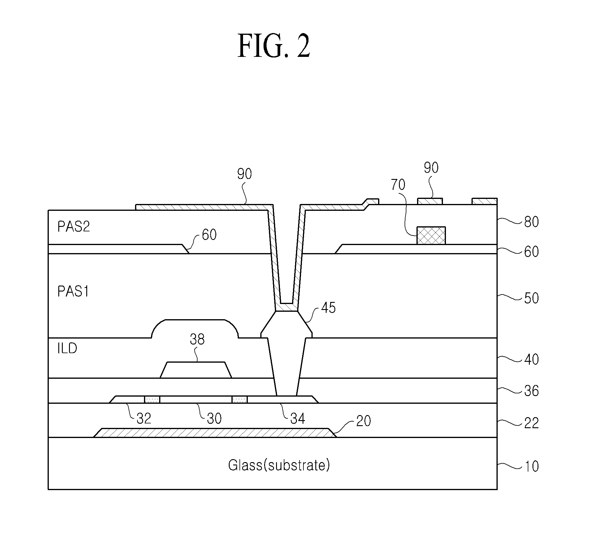
[0188]FIG. 16 is a view illustrating a pixel structure of an LCD device according to the present invention. In FIG. 16, a touch sensor is illustrated as being internalized in an in-cell touch type in the TFT array substrate. In FIG. 16, a color filter array substrate (upper substrate), a liquid crystal layer, a backlight unit, and a driving circuit part are not illustrated. The pixel structure of FIG. 8 is similar to that of FIG. 16, and thus, a detailed description on the same element is not provided.

[0189]Referring to FIG. 16, a TFT array substrate includes a glass substrate 110, a light shield 120, a buffer layer 122, a gate insulator 136, a data contact 145, a inter-layer dielectric (ILD) 140, a first passivation layer 150, a common electrode 160, a touch sensing line 170, a first contact line 160a, a second contact line 170a, a second passivation layer 180, a pixel electrode 190, and a TFT that includes an active 130, a source 132, an LDD 133, a drain 134, and a gate 138.

[0190]...


PUM

PropertyMeasurementUnit
sizeaaaaaaaaaa
lengthaaaaaaaaaa
widthaaaaaaaaaa

Abstract

Disclosed are an LCD device and a method of manufacturing the same, in which a passivation layer and a pixel electrode are simultaneously formed by a single mask process using a half tone mask, and thus, manufacturing efficiency increases, and a defective contact due to loss of the pixel electrode can be prevented in a pad area. The LCD device includes a pad part including a pad area and a contact area. The LCD device includes a pixel pad formed in the pad area, a pixel bar formed in the contact area, and a bridge layer contacting the pixel pad with the pixel bar. The bridge layer is formed as a single layer or multi layers, and formed of one or more of a transparent conductive material and an opaque conductive material.

Description

CROSS-REFERENCE TO RELATED APPLICATIONS[0001]This application claims the priority benefit of the Korean Patent Application No. 10-2011-0097759 filed on Sep. 27, 2011, and Korean Patent Application No. 10-2011-0097760 filed on Sep. 27, 2011, which is hereby incorporated by reference as if fully set forth herein.BACKGROUND[0002]1. Field of the Invention[0003]The present invention relates to a liquid crystal display (LCD) device, and more particularly, to an LCD device and a method of manufacturing the same, in which a passivation layer and a pixel electrode are simultaneously formed by a single mask process using a half tone mask, and thus, manufacturing efficiency increases, and a defective contact due to loss of the pixel electrode can be prevented in a pad area.[0004]2. Discussion of the Related Art[0005]Recently, in applying a touch sensor (screen) to LCD devices, a liquid crystal panel with integrated touch sensor is developed for slimming. Particularly, an in-cell touch type LCD...

Claims


Application Information

Patent Timeline
Patent Type & Authority Applications(United States)
IPC IPC(8): G02F1/1333H01J9/24
CPCG02F1/1345G02F1/13458G02F1/136227G06F3/0412H01L27/1244G02F2001/133357H01L27/1288G02F2001/136236G02F2001/13629G06F3/044G06F2203/04103H01L21/76802G02F2001/136231G06F3/0443G02F1/133357G02F1/136231G02F1/136236G02F1/13629G02F1/13452
Inventor JUNG, YOUNG KIYU, JAE SUNGSONG, IN HYUKPARK, JAE HOONLEE, HAN SEOK
Owner LG DISPLAY CO LTD
Why Eureka
Try Eureka