Semiconductor process

a technology of semiconductors and photomasks, applied in the direction of semiconductor devices, basic electric elements, electrical equipment, etc., can solve the problems of expensive and complicated use of two photomasks, and achieve the effect of simplifying the complicated process

Active Publication Date: 2013-03-28
UNITED MICROELECTRONICS CORP
View PDF10 Cites 24 Cited by
  • Summary
  • Abstract
  • Description
  • Claims
  • Application Information

AI Technical Summary

Benefits of technology

[0010]The present invention provides a semiconductor process, which entirely removes a metal layer in a recess while reserves a desired metal layer in the other recess by merely performing one time of a photolithography process; in other words, just using one photomask. Therefore, the present invention can simplify the complicated process of the prior art. Besides, due to the present invention does not using two photomasks, the scoring would not happen at the junction of the two photomasks, that leads to the material of the gate metal filling into the scoring and causing short circuit.

Problems solved by technology

However, using two photomasks is complicated and costly.

Method used


Image

  • Semiconductor process
  • Semiconductor process
  • Semiconductor process

Examples


Embodiment Construction

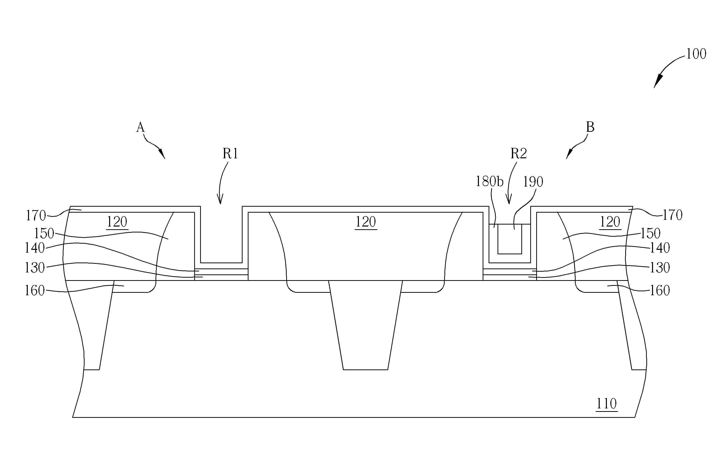
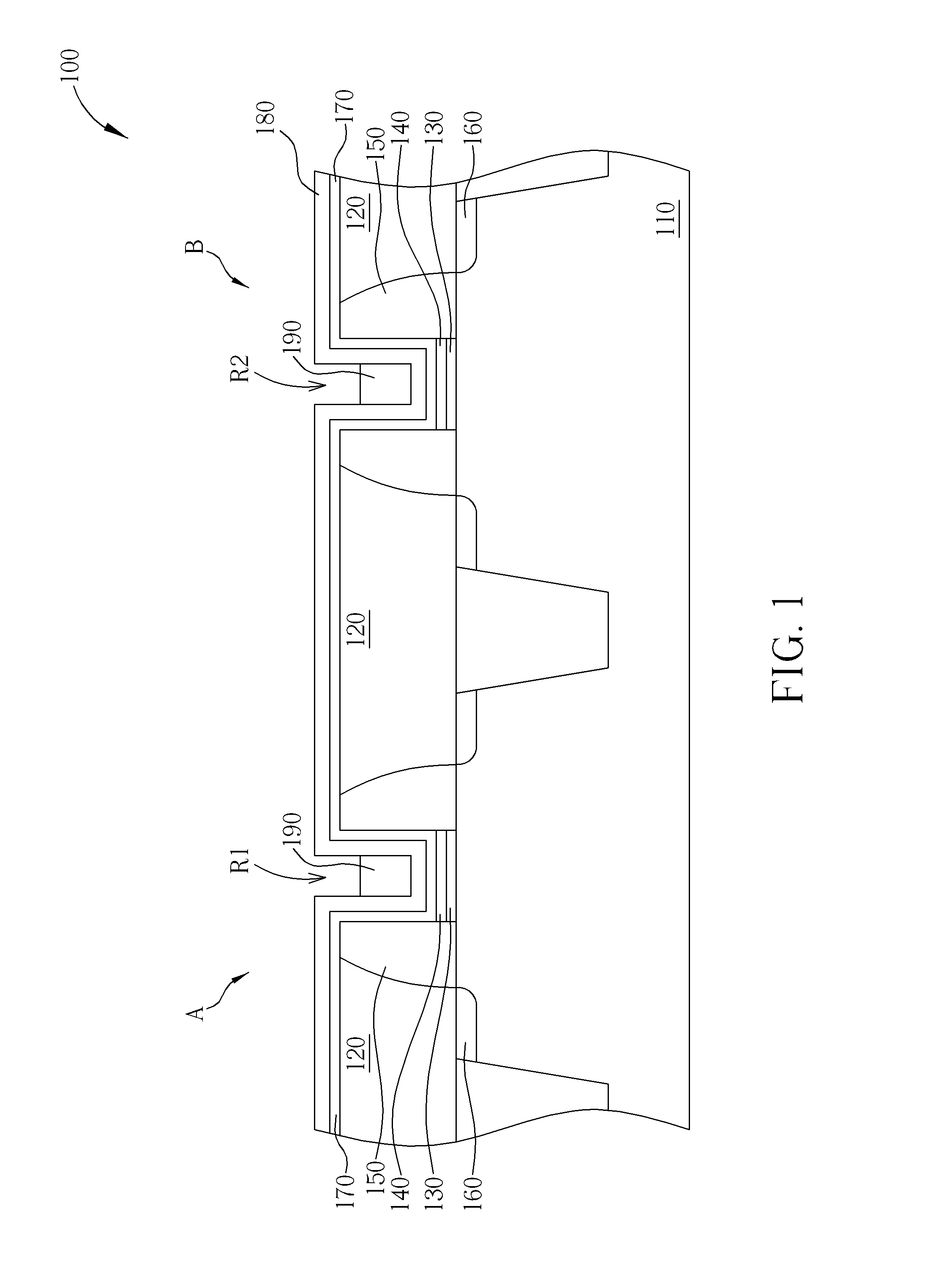
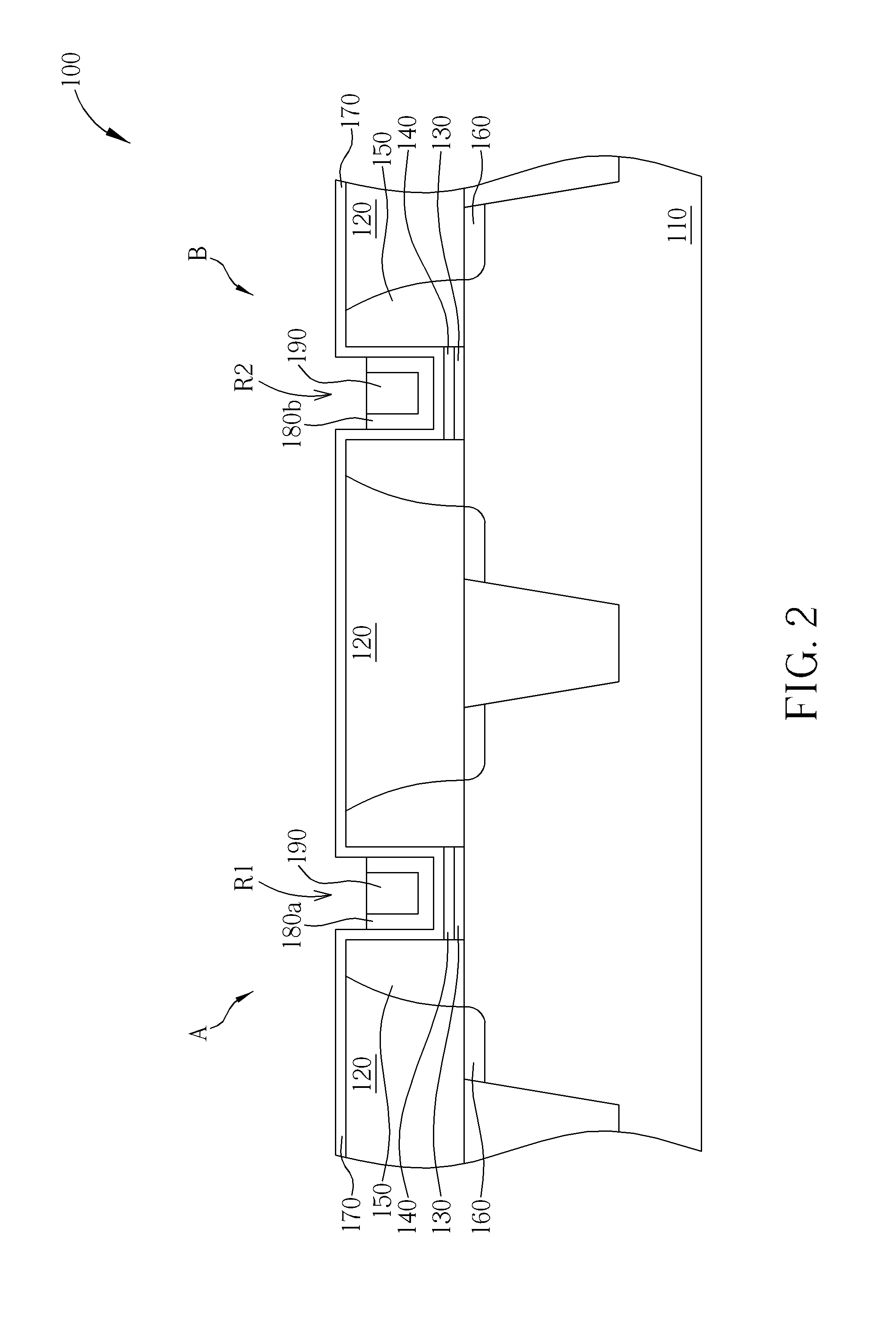
[0014]A CMOS transistor is used as an example in the two following embodiments, but the semiconductor process of the present invention can be also applied to other semiconductor components that are not described herein.

[0015]A gate-last for high-k first process is performed in the following example. FIGS. 1-6 schematically depict a cross-sectional view of a semiconductor process according to the first preferred embodiment of the present invention. As shown in FIG. 1, a substrate 110 is provided. A desired sacrificed gate (not shown) is formed, which may include an interlayer 130 being formed, a gate dielectric layer 140 being formed, a gate material layer (not shown) being formed and a cap layer (not shown) being formed, then the cap layer, the gate material layer, the gate dielectric layer 140, and the interlayer 130 being patterned to form the sacrificed gate. Then, a spacer 150 is formed, and a source / drain region 160 is formed beside the spacer 150 in the substrate 110. An inter...


PUM


Abstract

A semiconductor process includes the following steps. An interdielectric layer is formed on a substrate and the interdielectric layer has a first recess and a second recess. A metal layer is formed to cover the surface of the interdielectric layer, the first recess and the second recess. Partially fills a sacrificed material into the first recess and the second recess so that a portion of the metal layer in each of the recesses is respectively covered. The uncovered metal layer in each of the recesses is removed. The sacrificed material is removed. An etching process is performed to remove the remaining metal layer in the first recess and reserve the remaining metal layer in the second recess.

Description

BACKGROUND OF THE INVENTION[0001]1. Field of the Invention[0002]The present invention relates generally to a semiconductor process, and more specifically, to a semiconductor process in which only one photomask is used to form layers of different depths, such as metal layers, in two recesses.[0003]2. Description of the Prior Art[0004]In a complementary metal-oxide semiconductor (CMOS) device, a dual work function metal gate is used for both an NMOS device and a PMOS device. Integration and process controls for the dual work function metal gate are more complicated, while thickness and composition controls for materials used when fabricating the dual work function metal gate are more precise. Fabrication of the conventional dual work function metal gate can be categorized into gate first processes and gate last processes. In a conventional gate first process for fabricating a dual work function metal gate, both an annealing process for forming a source / drain ultra-shallow junction and...

Claims


Application Information

Patent Timeline
Patent Type & Authority Applications(United States)
IPC IPC(8): H01L21/28
CPCH01L21/28088H01L29/4966H01L21/823842H01L29/513H01L29/66545H01L29/51
Inventor HUANG, PONG-WEYYANG, CHAN-LONKUNG, CHANG-HUNGLIU, WEI-HSINHSIEH, YA-HSUEHLIAO, BOR-SHYANGHSUAN, TENG-CHUNYANG, CHUN-YAO
Owner UNITED MICROELECTRONICS CORP
Why Eureka
Try Eureka