
Integrated circuit with a self-programmed identification key

a self-programmed, integrated circuit technology, applied in the direction of capacitors, semiconductor/solid-state device details, instruments, etc., can solve the problems of counterfeiting of such circuits, difficult, or even impossible, to copy the chip having the same native code, and high cost for counterfeiters

Active Publication Date: 2013-04-04
STMICROELECTRONICS (CROLLES 2) SAS
View PDF2 Cites 22 Cited by
  • Summary
  • Abstract
  • Description
  • Claims
  • Application Information

AI Technical Summary

Benefits of technology

The patent describes a structure and method for storing a native binary code in an integrated circuit. This structure includes an array of capacitors connected to copper lines, with some of the capacitors having smaller breakdown voltages than others. The breakdown voltage of a capacitor is the minimum voltage needed to cause it to break down. The method involves connecting the capacitors in a particular way to cause a breakdown in a certain percentage of them. The breakdown voltage of the connected capacitors is lower than that of other capacitors. The structure can be used for secure authentication of the integrated circuit and as an identification number. The technical effect of this patent is a more secure and efficient way to store and access native binary codes in integrated circuits.

Problems solved by technology

The counterfeiting of such circuits thus is a major security issue regarding this so-called “hardware” approach.
Such fluctuations being in practice non-deterministic, a code which is generated based on such fluctuations would be pseudo-random and it would be difficult, or even impossible, to copy a chip having a same native code, short of replacing the corresponding circuit block with a block mimicking the original block and its code.
Such a strategy is theoretically possible but in practice very expensive for the counterfeiter, which makes it less advantageous.
Such a solution has the disadvantage that these values are continuous values and must be digitized to form a digital code exploitable by a program.
On the other hand, the aging and the degradation of the dielectric may result in an alteration of the code over time or according to the conditions of use of the circuit.
All these solutions have at least one of the two previously mentioned disadvantages, that is, they generate continuous analog values which must be previously digitized to obtain an exploitable binary code, or said code is unsteady by nature because it is sensitive to the aging of the circuit and to its conditions of use.

Method used


Image

  • Integrated circuit with a self-programmed identification key
  • Integrated circuit with a self-programmed identification key
  • Integrated circuit with a self-programmed identification key

Examples


Embodiment Construction

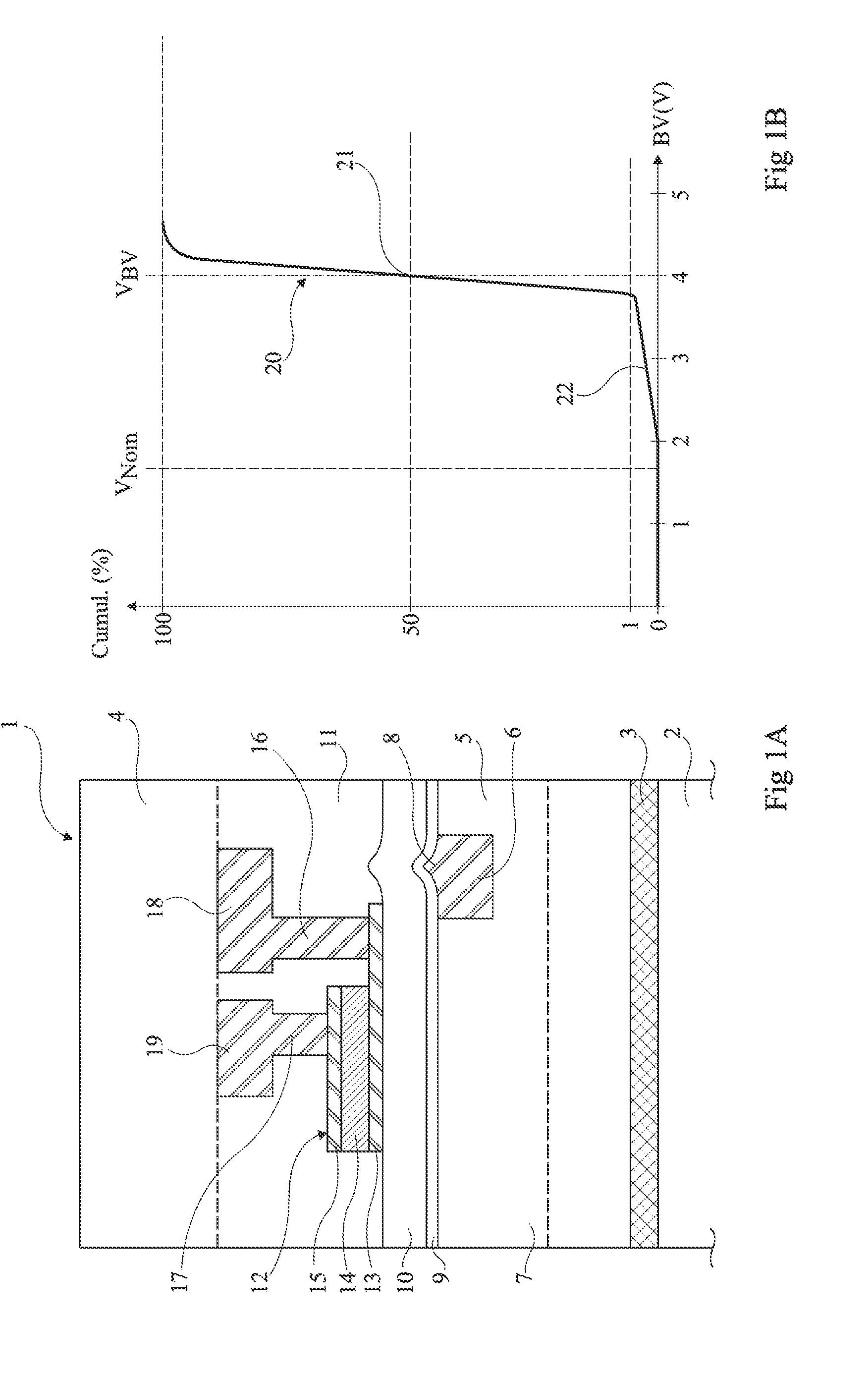
[0034]For clarity, the same elements have been designated with the same reference numerals in the different drawings and, further, as usual in the representation of integrated circuits, the various drawings are not to scale.

[0035]FIG. 1A is a cross-section view of an integrated circuit 1 comprising a planar metal-insulator-metal capacitor 12, known as a MIM capacitor. The integrated circuit comprises a semiconductor substrate 2 inside and on top of which active components 3, such as MOS transistors, topped with an assembly 4 of metallization levels, have been formed. The assembly 4 includes an intermediary metallization level 5 comprising a copper conductive line portion 6, formed in an insulating layer 7, for example, silicon oxide. A diffusion barrier layer 9, for example, made of silicon nitride, is interposed between metallization level 5 and the next metallization level 11 comprising a planar MIM capacitor 12. This capacitor is formed above a first insulating layer 10, for exam...


PUM


Abstract

A structure for storing a native binary code in an integrated circuit, including an array of planar MIM capacitors above an insulating layer formed above a copper metallization network, wherein at least one metallization portion is present under each MIM capacitor. The size of the portion(s) is selected so that from 25 to 75% of the MIM capacitors have a breakdown voltage smaller by at least 10% than that of the other MIM capacitors.

Description

BACKGROUND[0001]1. Technical Field[0002]The present disclosure relates to integrated circuits incorporating a code configured to identify or to authenticate the origin of these circuits. In particular, the present disclosure relates to integrated circuits for which this code is programmed in non-deterministic fashion, so that it is difficult or even impossible to make a copy of the integrated circuit including its code.[0003]2. Description of the Related Art[0004]Digital keys are especially exchanged over the Internet and used in identification protocols controlling financial transactions, the provision of e-services, contactless payments, the access to critical data, etc. To reinforce the security of such transactions, the digital keys are currently stored in a dedicated integrated circuit such as that of a chip card, for example, in an OTP-type (one-time programmable) non-volatile memory. One must then be physically in possession of this dedicated circuit to be authenticated. The ...

Claims


Application Information

Patent Timeline
IPC IPC(8): G11C17/04H01L21/02H01L27/10
CPCH01L23/5223H01L23/5252H01L23/544H01L23/576H01L28/40H01L2223/5444H01L2223/5448H01L2924/0002H01L2924/14H01L2924/00
Inventor PETITPREZ, EMMANUEL
Owner STMICROELECTRONICS (CROLLES 2) SAS
Learn More