Heating element mounting substrate, method of manufacturing the same and semiconductor package

Inactive Publication Date: 2013-04-11
HITACHI CABLE
View PDF0 Cites 6 Cited by
  • Summary
  • Abstract
  • Description
  • Claims
  • Application Information

AI Technical Summary

Benefits of technology

[0033]According to one embodiment of the invention, a heating element mounting substrate can be provided that is a single-sided printed circuit board but has good thermal conductivity in a plate thickness direction and versatility allowing conductive patterns exposed on both surfaces to be designed in different shapes, as well as a method of manufacturing the heating element mounting substrate and a semicond

Problems solved by technology

However, there are problems that thermal resistance of the resin substrate in a thickness direction is likely to become large and the ceram

Method used


Image

  • Heating element mounting substrate, method of manufacturing the same and semiconductor package
  • Heating element mounting substrate, method of manufacturing the same and semiconductor package
  • Heating element mounting substrate, method of manufacturing the same and semiconductor package

Examples


Example

First Embodiment

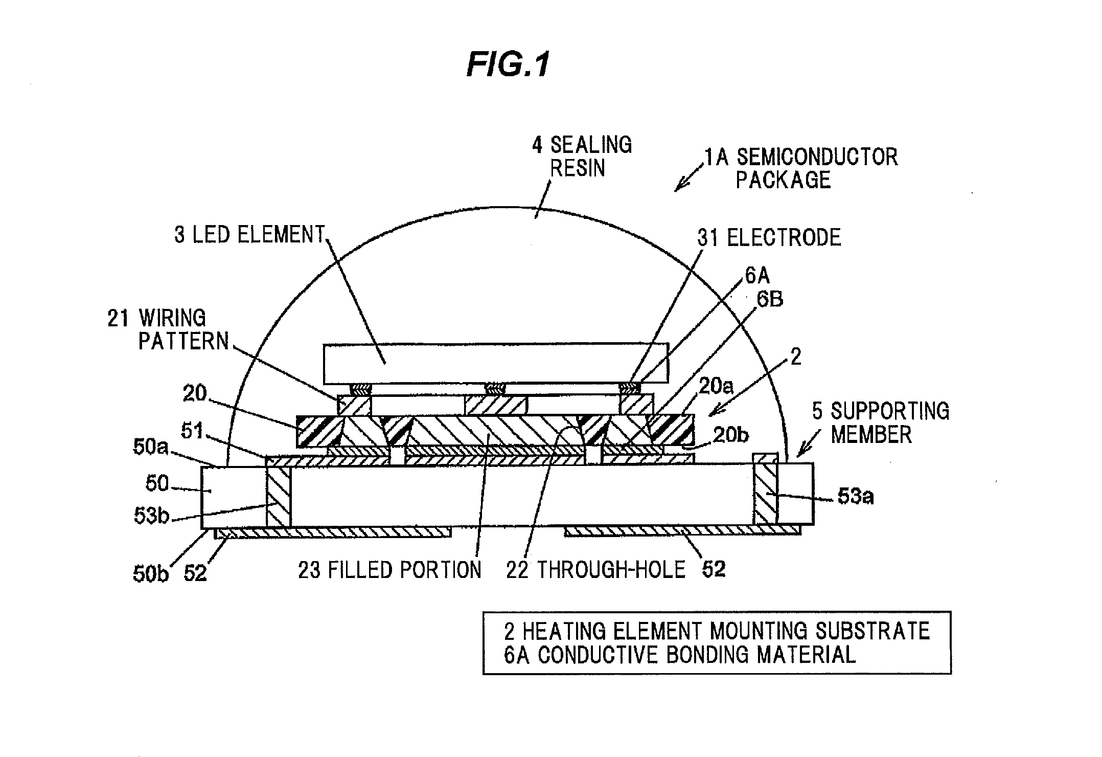
[0051]FIG. 1 is a cross sectional view showing a semiconductor package in a first embodiment of the invention. For forming a semiconductor package 1A, an LED element 3 is flip-chip mounted on a heating element mounting substrate 2, the heating element mounting substrate 2 mounting the LED element 3 thereon is mounted on a supporting member 5 and the LED element3 is sealed with a sealing resin 4.

[0052]Heating Element Mounting Substrate

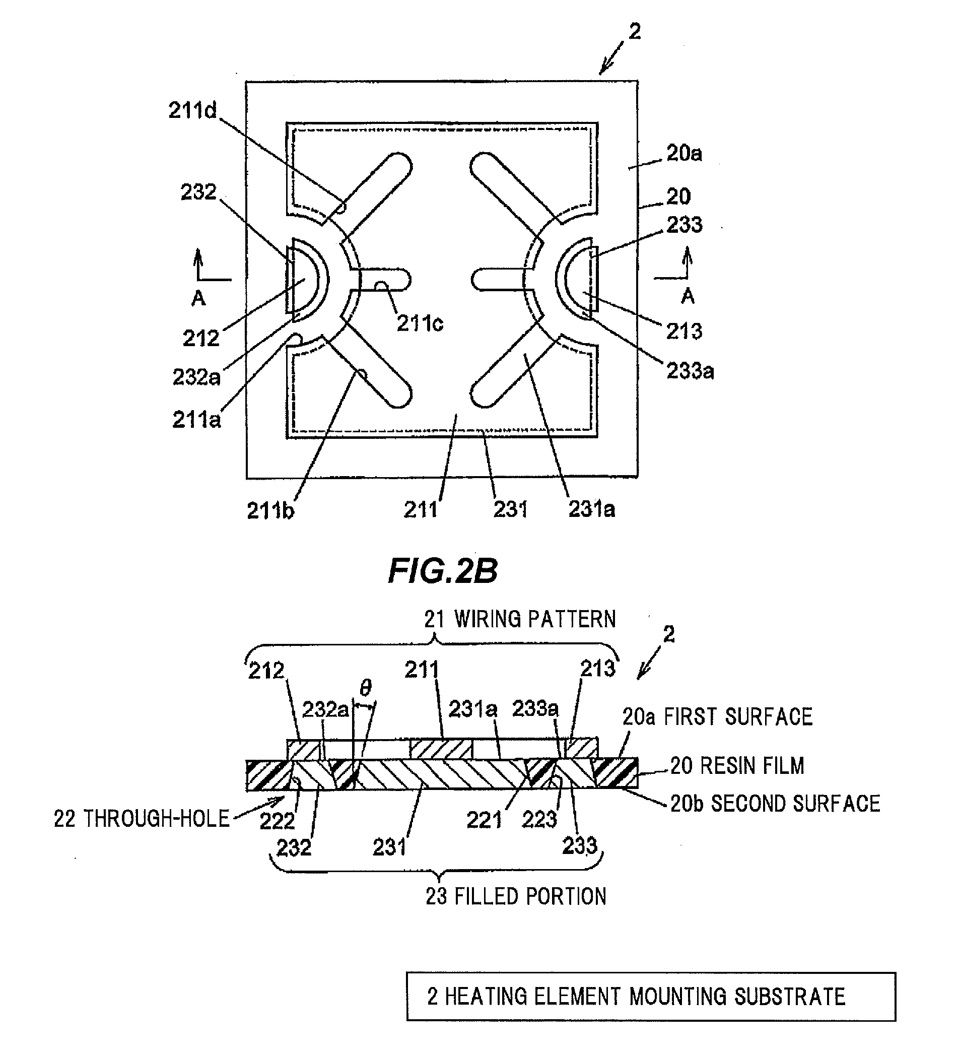
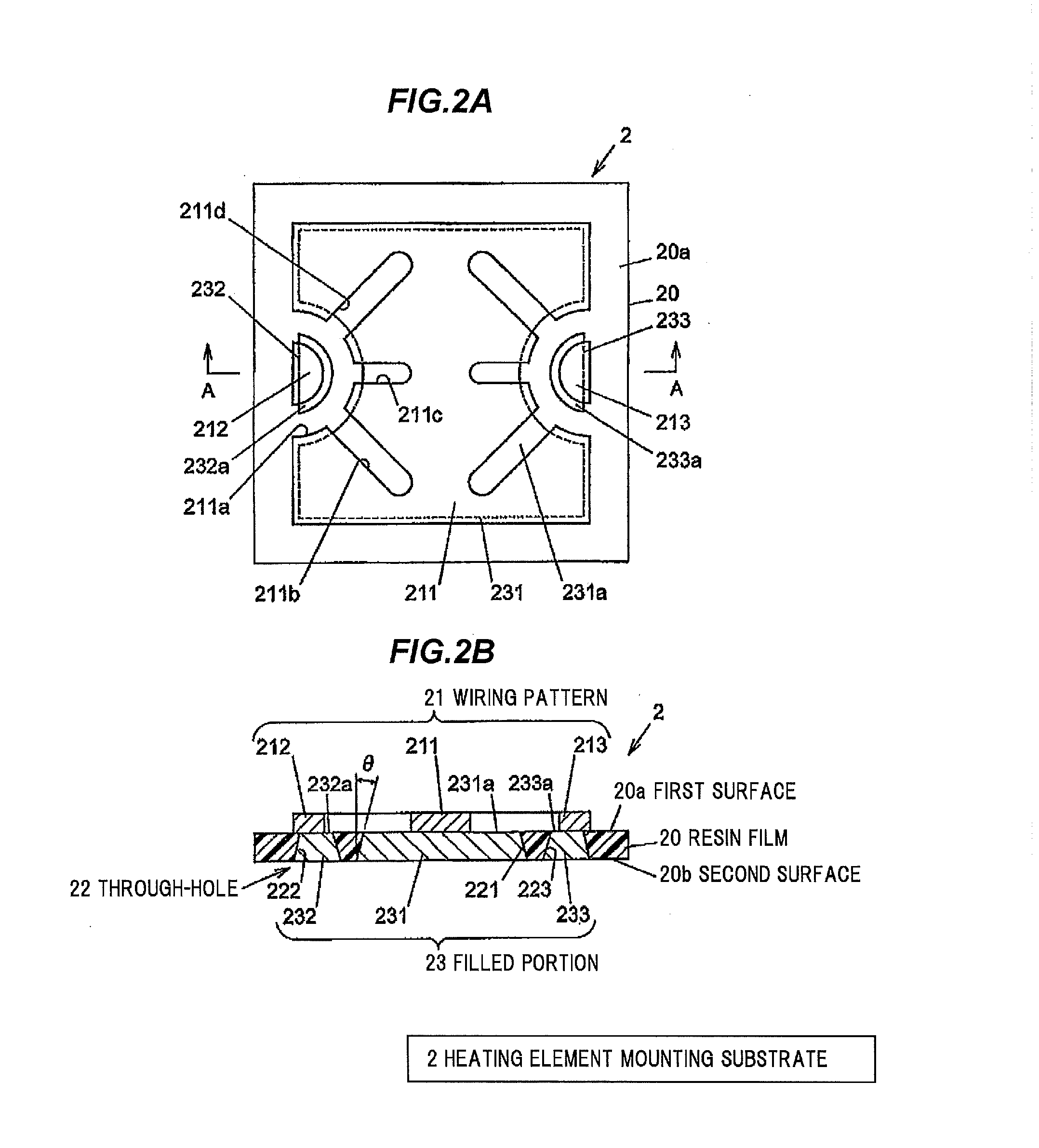
[0053]FIGS. 2A and 2B show a heating element mounting substrate 2, wherein FIG. 2A is a plan view and FIG. 2B is a cross sectional view taken on line A-A of FIG. 2A. The heating element mounting substrate 2 is a so-called single-sided printed circuit board having a wiring on one surface of a substrate, and is provided with a resin film 20 having a first surface 20a and a second surface 20b opposite to the first surface 20a, wiring patterns 21 (211, 212 and 213) formed on the first surface 20a of the resin film 20, and filled portions 23 ...

Example

Second Embodiment

[0095]FIG. 7 is a cross sectional view showing a semiconductor package in a second embodiment of the invention. A semiconductor package 1B is configured in the same manner as the first embodiment except that the heating element mounting substrate 2 is arranged upside down.

[0096]That is, in the semiconductor package 1B of the second embodiment, the wiring patterns 21 of the heating element mounting substrate 2 are connected to the front-surface wiring pattern 51 of the ceramic substrate 50 by the conductive bonding material 6B and the LED element 3 is flip-chip mounted on the filled portions 23 of the heating element mounting substrate 2 via the conductive bonding material 6A. The LED element 3 is mounted on the second surface 20b of the heating element mounting substrate 2 (resin film 20).

[0097]In the second embodiment, it is possible to manufacture in the same manner as the first embodiment. In other words, the heating element mounting substrate 2 is made in the sa...

Example

Third Embodiment

[0104]FIG. 9 is a cross sectional view showing a semiconductor package in a third embodiment of the invention. FIG. 10 is a cross sectional view showing a state in which an LED element is flip-chip mounted on a heating element mounting substrate in the third embodiment. A semiconductor package 1C is configured in the same manner as the second embodiment except that the filled portion 23 has a two-layer structure.

[0105]In the heating element mounting substrate 2 of the third embodiment, the filled portion 23 is filled in the through-hole 22 of the resin film 20 up to half or more of the thickness of the resin film 20 and the remaining portion of the through-hole 22 is filled with the conductive bonding material 6C as shown in FIG. 10. Alternatively, the filled portion 23 may be about half or not more than half of the thickness of the resin film 20.

[0106]In the semiconductor package 1C of the third embodiment, the wiring patterns 21 of the heating element mounting subs...


PUM


Abstract

A heating element mounting substrate includes a substrate including a first surface and a second surface, a plurality of wiring patterns formed on the first surface of the substrate, and a plurality of filled portions including a conductive material filled in a plurality of through-holes, the plurality of through-holes penetrating through the substrate in a thickness direction. At least one of the plurality of wiring patterns has an area of not less than 30% of an area of the first surface of the substrate. The plurality of filled portions includes non-overlapping portions that extend from the plurality of wiring patterns as viewed from the first surface side of the substrate, areas of the plurality of filled portions overlapped with the plurality of wiring patterns are not less than 50% of respective areas of the corresponding wiring patterns as viewed from the second surface side of the substrate.

Description

[0001]The present application is based on Japanese patent application Nos. 2011-222966 and 2012-203970 filed on Oct. 7, 2011 and Sep. 18, 2012, respectively, the entire contents of which are incorporated herein by reference.BACKGROUND OF THE INVENTION[0002]1. Field of the Invention[0003]The invention relates to a heating element mounting substrate for mounting a heating element, a method of manufacturing the heating element mounting substrate, and a semiconductor package using the heating element mounting substrate.[0004]2. Related Art[0005]Among heating elements (elements accompanied by heat generation), LED (Light Emitting Diode) elements have recently attracted a lot of attention from the viewpoint of energy saving and CO2 reduction. In particular, flip-chip type LED elements having electrodes all arranged on the same surface are considered to be advantageous to improve luminous efficiency (1 m / W) since electrodes and wires can be cleared from a main light-emitting surface side, ...

Claims


Application Information

Patent Timeline
IPC IPC(8): H05K1/00H05K3/10
CPCH01L33/62H01L33/641H01L33/647H05K1/0206H01L2224/16225H01L2933/0075H05K2201/10106
Inventor IMAI, NOBORUISAKA, FUMIYAMATSUO, NAGAYOSHINEMOTO, MANSANORITANOI, MINORU
Owner HITACHI CABLE
Why Eureka
Try Eureka