
Thin film transistor substrate and liquid crystal display device

a technology of thin film transistors and substrates, applied in semiconductor devices, instruments, electrical devices, etc., can solve problems such as flickering and fluctuation of screen brightness, and achieve the effects of reducing the power consumption of backlight, preventing flickering, and reducing the potential change at the pixel electrodes

Inactive Publication Date: 2013-04-11
SHARP KK
View PDF6 Cites 15 Cited by
  • Summary
  • Abstract
  • Description
  • Claims
  • Application Information

AI Technical Summary

Benefits of technology

The present invention provides a new design that reduces power consumption and prevents flickering in a display by using a transparent conductive material to shield the pixel electrodes from potential changes. This is achieved by extending a shielding electrode along both wiring lines and between the two wiring lines and the pixel electrodes. This results in a reduction in power consumption while maintaining the desired display quality, even with low-frequency driving.

Problems solved by technology

In the TFT substrate having such a structure, a parasitic capacitance is formed between the gate wiring lines or the source wiring lines and the pixel electrodes due to a potential difference therebetween, and therefore, the potential at the pixel electrodes changes in accordance with the permittivity of the interlayer insulating film disposed between these wiring lines and the pixel electrode, causing fluctuations of the screen brightness, i.e., flickering.

Method used


Image

  • Thin film transistor substrate and liquid crystal display device
  • Thin film transistor substrate and liquid crystal display device
  • Thin film transistor substrate and liquid crystal display device

Examples


Embodiment Construction

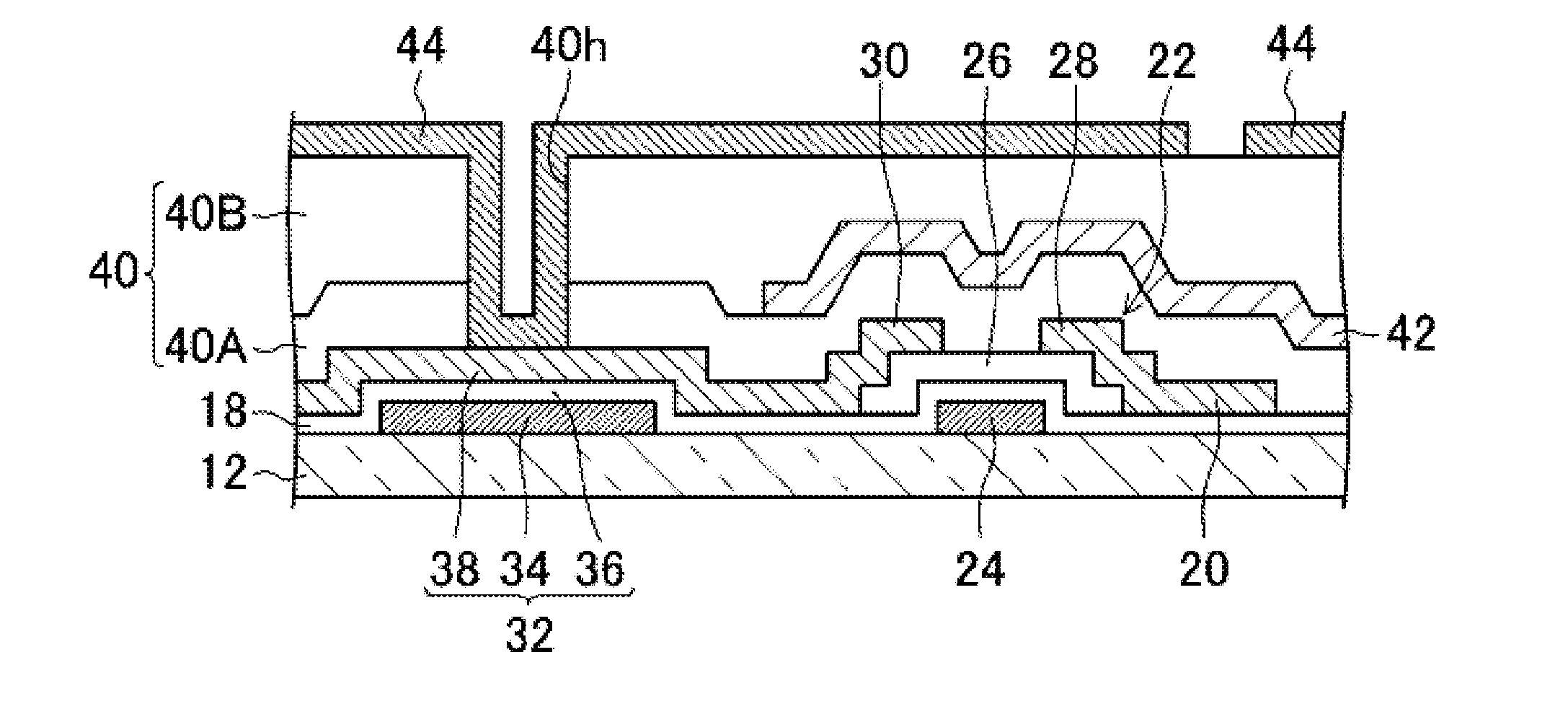
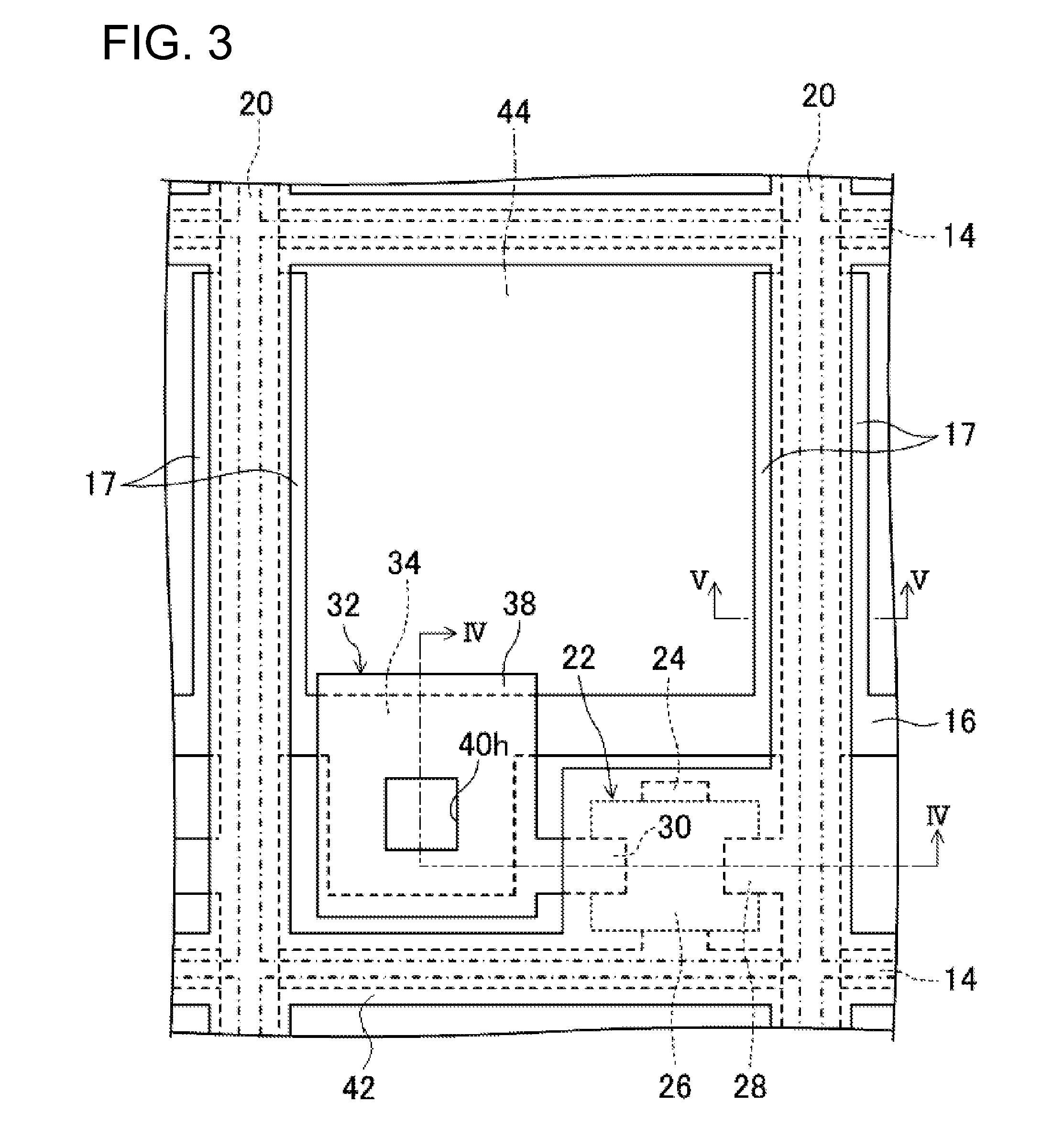
[0037]Below, an embodiment of the present invention will be explained in detail with reference to figures. The present invention is not limited to the embodiment described below.

Embodiment of the Present Invention

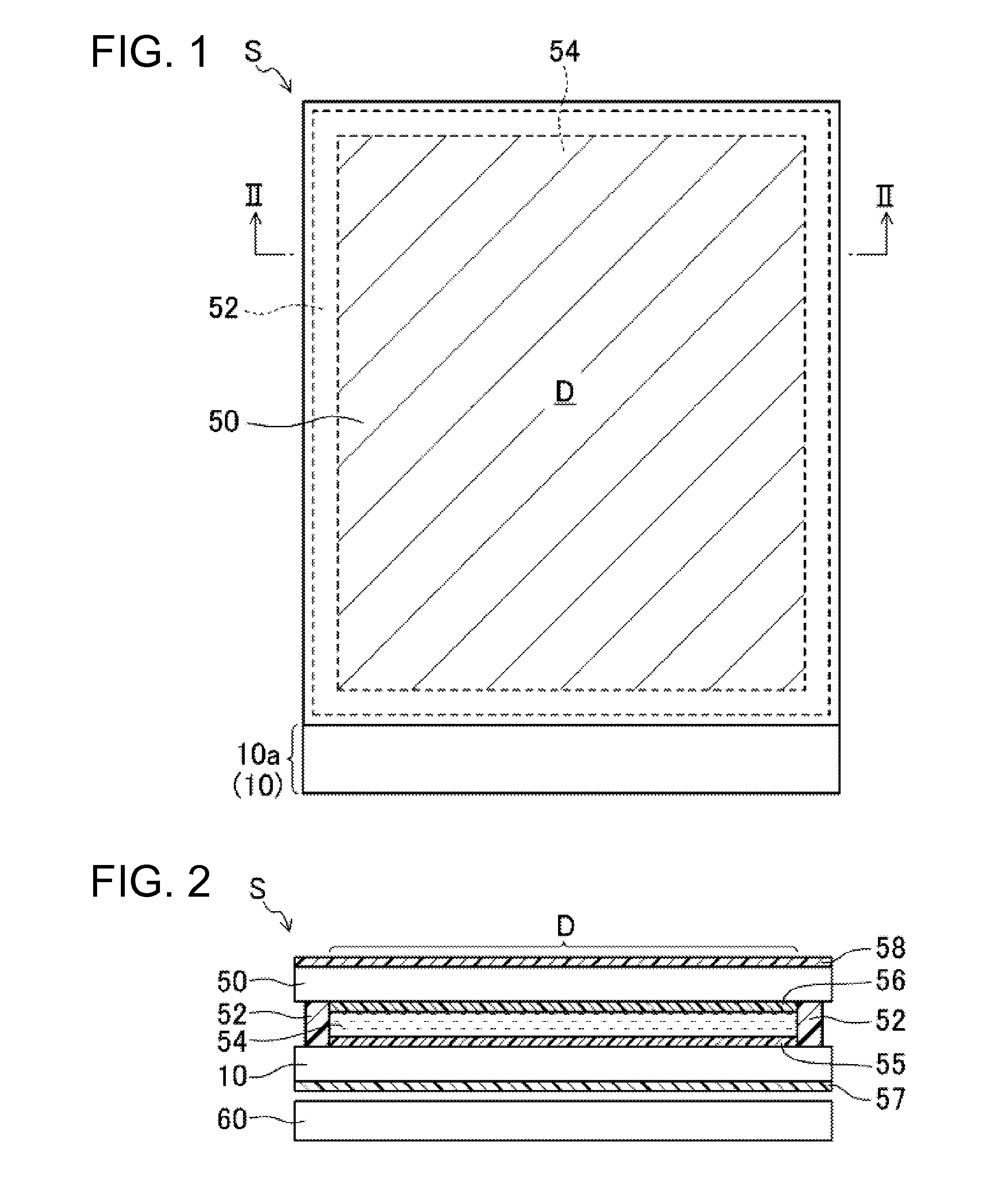
[0038]FIG. 1 is a schematic plan view of a liquid crystal display device S according to this embodiment. FIG. 2 is a schematic cross-sectional view showing a cross-sectional structure along the line II-II in FIG. 1. In FIG. 1, a polarizing plate 58 shown in FIG. 2 is not shown.

[0039]

[0040]The liquid crystal display device S is a transmissive liquid crystal display device that includes a TFT substrate 10 and an opposite substrate 50 disposed to face each other, a frame-shaped sealing member 52 that bonds the TFT substrate 10 and the opposite substrate 50 to each other in the respective outer edge portions thereof, a liquid crystal layer 54 sealed inside the sealing member 52 between the TFT substrate 10 and the opposite substrate 50, and a backlight 60 disposed on the rear s...


PUM


Abstract

Disclosed is a liquid crystal display device including a thin film transistor substrate, in which changes in the potential at a pixel electrode can be suppressed without decreasing the aperture ratio of a pixel. Gate wiring lines and source wiring lines are covered with a multilayer insulating film made of two layers of interlayer insulating films that overlap each other. Pixel electrodes are formed on the multilayer insulating film, and a shield electrode, which is formed of a transparent conductive material, is provided between the two layers of interlayer insulating films so as to extend along the gate wiring lines and the source wiring lines and to lie between the gate electrodes or the source electrodes and the pixel electrodes.

Description

TECHNICAL FIELD[0001]The present invention relates to a thin film transistor (referred to as a TFT below) substrate and to a liquid crystal display device provided with the same, and more particularly, to a countermeasure against fluctuations in the screen brightness, i.e., flickering, to achieve a reduction in power consumption by low-frequency driving.BACKGROUND ART[0002]An active matrix driving type liquid crystal display device has a structure in which a liquid crystal layer is sealed between a TFT substrate and an opposite substrate facing each other, and by having TFTs in respective pixels, each of which is the smallest unit of an image, the liquid crystal display device can display high-resolution images.[0003]The TFT substrate includes a plurality of gate wiring lines that extend in parallel with each other, a plurality of source wiring lines that extend in parallel with each other so as to intersect with the respective gate wiring lines, and TFTs and pixel electrodes that a...

Claims


Application Information

Patent Timeline
Patent Type & Authority Applications(United States)
IPC IPC(8): H01L27/15
CPCG02F1/133345G02F1/1362H01L27/124H01L27/15H01L27/1255G02F2001/136218G02F1/136218
Inventor KANEKO, SEIJI
Owner SHARP KK
Features
  • Generate Ideas
  • Intellectual Property
  • Life Sciences
  • Materials
  • Tech Scout
  • Unparalleled Data Quality
  • Higher Quality Content
  • 60% Fewer Hallucinations
Learn More