Cable for high-voltage electronic devices

a high-voltage electronic device and cable technology, applied in the field of cables, can solve the problems of dielectric breakdown, large resistivity drop, insufficient withstand voltage characteristics, etc., and achieve the effect of excellent withstand voltage characteristics and small diameter

Active Publication Date: 2013-04-18
VAREX IMAGING NEDERLAND BV
View PDF4 Cites 12 Cited by
  • Summary
  • Abstract
  • Description
  • Claims
  • Application Information

AI Technical Summary

Benefits of technology

[0017]According to one embodiment of the present invention, it is possible to obtain a cable for high-voltage electronic devices that is small in diameter yet has an excellent withstand voltage characteristic.

Problems solved by technology

These EP rubber compositions, however, have a problem that their withstand voltage characteristic is not high enough because their volume resistivity greatly lowers as temperature increases due to high temperature dependence of the volume resistivity.
As a result, an electric field concentrates near an interface between the outer semiconductive layer and the high-voltage insulator, which tends to cause dielectric breakdown.
This phenomenon also occurs in an AC power cable, but causes a great problem especially in a DC power cable such as a cable for high-voltage electronic devices.
This phenomenon causes a still greater problem in a cable realizing a diameter reduction by the use of the low-dielectric constant EP rubber composition because its high-voltage insulator is thin.

Method used


Image

  • Cable for high-voltage electronic devices
  • Cable for high-voltage electronic devices

Examples


example 1

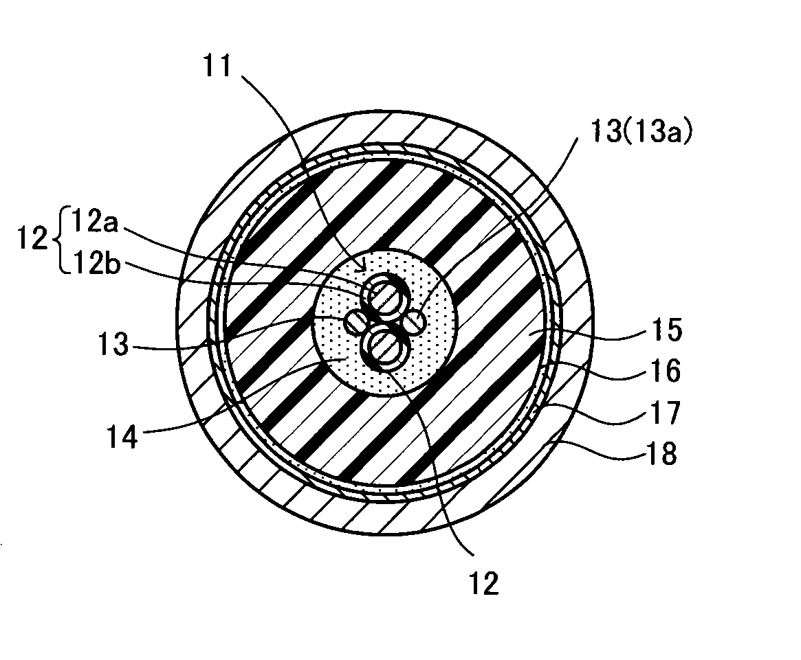
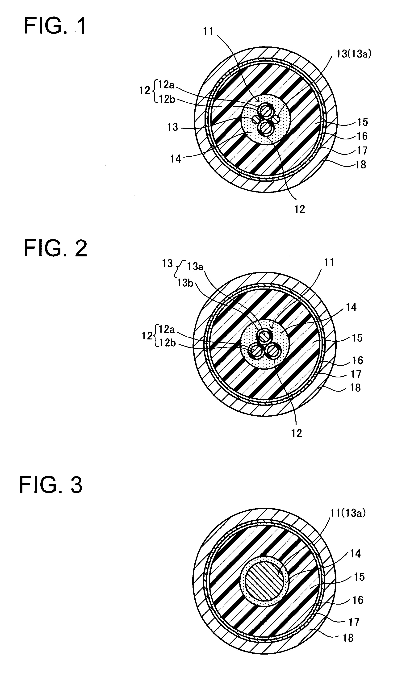
[0053]Two low-voltage cable cores each coated with an insulator formed of polytetrafluoroethylene and having a 0.25 mm thickness and two high-voltage cable cores each composed of a bare conductor with a 1.25 mm2 sectional area which was formed by collective stranding of 50 tin-plated annealed copper wires each having a 0.18 mm diameter were stranded on a conductor having a 1.8 mm2 sectional area which was formed by collective stranding of 19 tin-plated annealed copper wires each having a 0.35 mm diameter, whereby a cable core part was formed. A semiconductive tape formed of a nylon base material was wound around an outer periphery of the cable core part to form an inner semiconductive layer having a thickness of about 0.5 mm.

[0054]An insulating composition, which was prepared by uniformly kneading 100 parts by mass of EPDM (Mitsui EPT #1045, trade name, manufactured by Mitsui Chemicals, Inc.), 0.5 part by mass of dry silica with a 200 m2 / g specific surface area (BET method), a 4.2 p...

examples 2 , 3

Examples 2, 3, Comparative Examples 1 to 4

[0055]Cables for high-voltage electronic devices were produced in the same manner as in the example 1 except that the compositions of forming materials of the high-voltage insulator were changed as shown in Table 1. Dry silicas used besides the dry silica (a) are as follows.

[0056]dry silica (b): specific surface area (BET method) 100 m2 / g, ph 4.2, average primary-particle diameter 10 nm

[0057]dry silica (c): specific surface area (BET method) 300 m2 / g, ph 4.0, average primary-particle diameter 12 nm

[0058]Regarding the cables for high-voltage electronic devices obtained in the examples and the comparative examples, capacitance and a withstand voltage characteristic were measured or evaluated by the following methods.

[Capacitance]

[0059]This was measured by a high-voltage Schering bridge method under conditions of 1 kV and a 50 Hz frequency.

[Withstand Voltage Characteristic]

[0060]A 200 kV DC voltage was applied for ten minutes, and acceptance ju...


PUM

PropertyMeasurementUnit
specific surface areaaaaaaaaaaa
average primary-particle diameteraaaaaaaaaa

Abstract

A cable for high-voltage electronic devices including an inner semiconductive layer, a high-voltage insulator, an outer semiconductive layer, a shielding layer, and a sheath which are provided on an outer periphery of a cable core part in the order mentioned, wherein the high-voltage insulator is made of an insulating composition whose temperature dependence parameter DR found by the following expression is 1.0 or less: DR=log R23° C.−log R90° C. (where R23° C. is volume resistivity (Ω·cm) at 23° C. and R90° C. is volume resistivity (Ω·cm) at 90° C.). The cable for high-voltage electronic devices is small in diameter and has an excellent withstand voltage characteristic.

Description

TECHNICAL FIELD[0001]The present invention relates to a cable used for high-voltage electronic devices such as CT (computerized tomography) devices for medical use and X-ray devices.BACKGROUND ART[0002]Cables for high-voltage electronic devices such as CT devices for medical use and X-ray devices to which a high DC voltage is applied are required (i) to be small in outside diameter and light-weighted, (ii) to have good flexibility and be resistant against movement and bending, (iii) to be small in capacitance and be capable of following the repeated application of high-voltages, and (iv) to have heat resistance high enough to endure the heat generation of an X-ray vacuum tube part.[0003]As such a cable for high-voltage electronic devices (for example, an X-ray cable), there has been known one in which two low-voltage cable cores and one bare conductor or two are twisted together, an inner semiconductive layer is provided thereon, and a high-voltage insulator, an outer semiconductive...

Claims


Application Information

Patent Timeline
Patent Type & Authority Applications(United States)
IPC IPC(8): H01B9/02
CPCH01B3/28H01B9/027H01B3/441
Inventor SAITO, MARIKOMINOWA, MASAHIROYAMAGUCHI, MASAMITSUNOGUTI, KAZUAKI
Owner VAREX IMAGING NEDERLAND BV
Why Eureka
Try Eureka