Structure of semiconductor chips with enhanced die strength and a fabrication method thereof

a technology of enhanced die strength and semiconductor chips, which is applied in the direction of semiconductor devices, semiconductor/solid-state device details, electrical devices, etc., can solve the problems of high probability of die cracking, insufficient die strength, and damage to the function of integrated circuits in the active layer, so as to improve the fabrication tool capacity and improve the structure of semiconductor chips. , the effect of enhancing die strength

Inactive Publication Date: 2013-04-25
WIN SEMICON
View PDF5 Cites 5 Cited by
  • Summary
  • Abstract
  • Description
  • Claims
  • Application Information

AI Technical Summary

Benefits of technology

[0006]The main object of the present invention is to provide an improved structure of semiconductor chips with enhanced die strength and a fabrication method thereof, in which a backside metal layer is deposited directly to fully cover the backside of a substrate. The street masking step in the previous technology can be eliminated. Thereby the fabrication tool capacity can be increased, and the process cycle time can be reduced to nearly half. The fabrication cost can therefore be significantly reduced.
[0007]Another object of the present invention is to provide an improved structure of semiconductor chips with enhanced die strength and a fabrication method thereof, in which, before depositing a backside metal layer to the backside of a substrate, the backside of the substrate can be thinned first. The substrate can be thinned to have a thickness less than 50 μm. Consequently, when drilling, dry etching, or any further processing is applied to the substrate, the process cycle time can be significantly reduced. The processing tool capacity can be increased and the depletion of the processing tools can be decreased. The fabrication cost can therefore be significantly reduced.
[0008]Another object of the present invention is to provide an improved structure of semiconductor chips with enhanced die strength and a fabrication method thereof, in which a backside metal layer is deposited directly to fully cover the backside of a substrate. By applying the specific dicing process of the present invention, the backside metal layer and the substrate can be diced tidily. Die cracking on the border between the substrate and the backside metal layer of a single chip after dicing can be prevented and thereby the die strength can be significantly enhanced

Problems solved by technology

Moreover, the metal fragments may adhere to the integrated circuits in the active layer 103, which will damage the function of integrated circuits in the active layer 103.
Thereby, the die strength is often insufficient, which leads to high probability of the occurrence of die-crack.

Method used


Image

  • Structure of semiconductor chips with enhanced die strength and a fabrication method thereof
  • Structure of semiconductor chips with enhanced die strength and a fabrication method thereof
  • Structure of semiconductor chips with enhanced die strength and a fabrication method thereof

Examples


Embodiment Construction

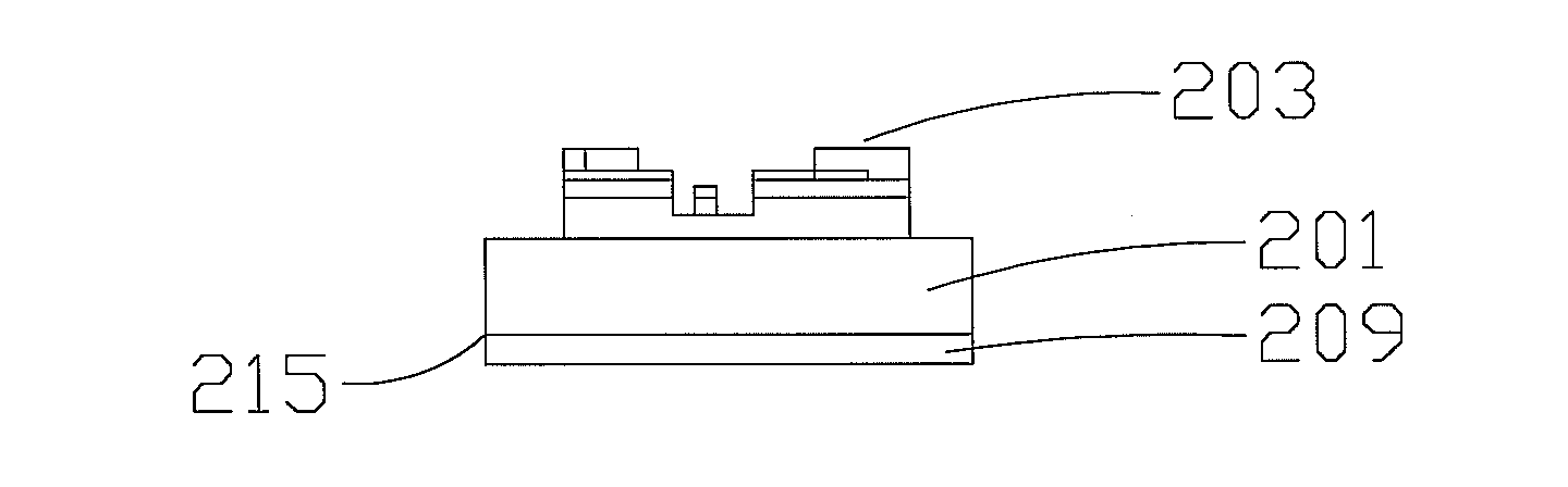
[0031]FIG. 2A is a cross-sectional view of the structure of the substrate of integrated circuit chips of the present invention before back thinning, which comprises a substrate 201; an active layer 203 disposed above the substrate 201. The substrate 201 is formed preferably of GaAs, SiC, GaN, Si or InP. The active layer 203 includes at least one integrated circuit. In an embodiment, the active layer 203 usually includes multiple independent integrated circuits, which will be cut into multiple independent integrated circuit chips and then packaged to make product. A backside metal layer has to be deposited to the backside of the substrate 201 before dicing, which can enhance the die strength on one hand, and facilitate the adhesion in packaging on the other hand. In an embodiment, before depositing a backside metal layer to the backside of the substrate 201, the backside of the substrate 201 will be thinned first. The thickness of the substrate 201 is preferably larger than 10 μm and...


PUM


Abstract

An improved structure of semiconductor chips with enhanced die strength and a fabrication method thereof are disclosed. The improved structure comprises a substrate, an active layer, and a backside metal layer, in which the active layer is formed on the front side of the substrate and includes at least one integrated circuit; the backside metal layer is formed on the backside of the substrate, which fully covers the area corresponding to the area covered by the integrated circuits in the active layer. By using the specific dicing process of the present invention, the backside metal layer and the substrate can be diced tidily. Die cracking on the border between the substrate and the backside metal layer of the diced single chip can be prevented, and thereby the die strength can be significantly enhanced.

Description

FIELD OF THE INVENTION[0001]The present invention relates to an improved structure of semiconductor chips with enhanced die strength and a fabrication method thereof, in particular to an improved structure of semiconductor chips with enhanced die strength and a fabrication method thereof without beforehand back-etching of masking streets of the substrate, the substrate thereof is first thinned to have a thickness less than 100 μm, and then a backside metal layer is deposited to the backside of the substrate. By using the specific dicing process of the present invention, the chips can be diced tidily. The fabrication tool capacity can be increased; the process cycle time can be reduced to nearly half; the usage of material can be reduced; the efficiency of heat dissipation of the diced single chip can be increased; and the die strength can be significantly enhanced.BACKGROUND OF THE INVENTION[0002]FIG. 1A are schematics showing the front and the back views of the substrate of integra...

Claims


Application Information

Patent Timeline
Patent Type & Authority Applications(United States)
IPC IPC(8): H01L29/16H01L29/20H01L21/78H01L23/48
CPCH01L23/562H01L23/4827H01L2924/0002H01L29/0657H01L2924/00
Inventor HUA, CHANG-HWANG
Owner WIN SEMICON
Why Eureka
Try Eureka