Recessed Single Crystalline Source and Drain For Semiconductor-On-Insulator Devices

a single crystalline source and semiconductor technology, applied in the field of semiconductor structures, can solve the problems of affecting the performance of field effect transistors, high drain resistance adversely affecting the performance of devices formed on semiconductor-on-insulator (soi) substrates having a thin top semiconductor layer, and prone to performance degradation, so as to reduce parasitic capacitive coupling, reduce drain resistance, and improve the overall performance of etsoi devices.

Active Publication Date: 2013-05-02
GLOBALFOUNDRIES US INC
View PDF0 Cites 19 Cited by
  • Summary
  • Abstract
  • Description
  • Claims
  • Application Information

AI Technical Summary

Benefits of technology

[0003]A semiconductor-on-insulator (SOI) substrate including a buried single crystalline rare earth oxide layer is provided. The buried single crystalline rare earth oxide layer includes a single crystalline layer of an oxide of at least one rare earth element, and has a lattice constant that is compatible with epitaxial growth of a single crystalline semiconductor material thereupon. After formation of a gate stack on the top semiconductor layer of the SOI substrate, regions in which a source and a drain are to be formed are recessed through the top semiconductor layer and into an upper portion of the buried single crystalline rare earth oxide layer. A source trench and drain t...

Problems solved by technology

High source resistance or high drain resistance adversely impacts the performance of a field effect transistor by limiting the on-current of the field effect transistor.
Thus, devices formed on a semiconductor-on-insulator (SOI) substrate having a thin top semiconductor layer is prone to performance degradation due to redu...

Method used


Image

  • Recessed Single Crystalline Source and Drain For Semiconductor-On-Insulator Devices
  • Recessed Single Crystalline Source and Drain For Semiconductor-On-Insulator Devices
  • Recessed Single Crystalline Source and Drain For Semiconductor-On-Insulator Devices

Examples


first embodiment

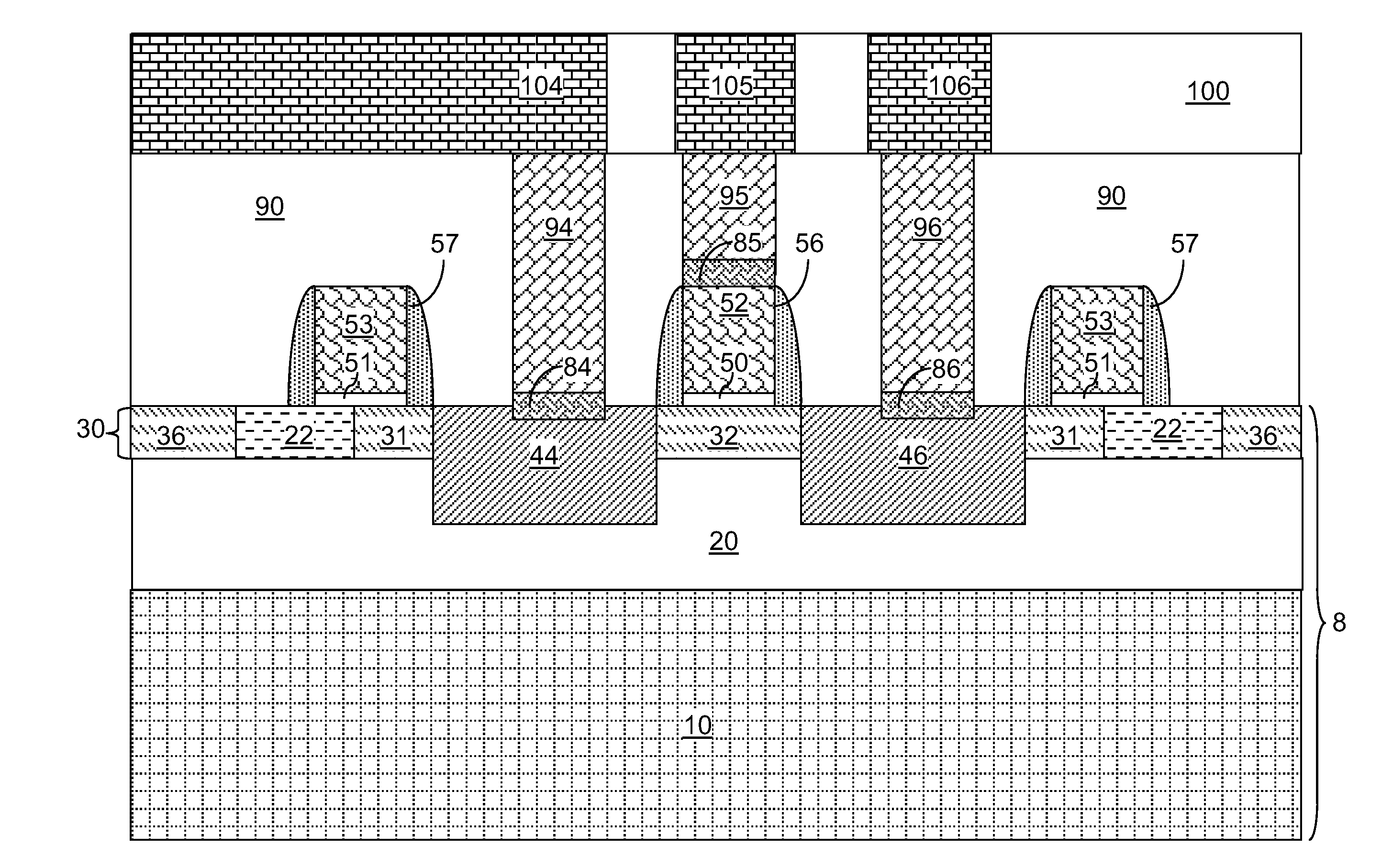
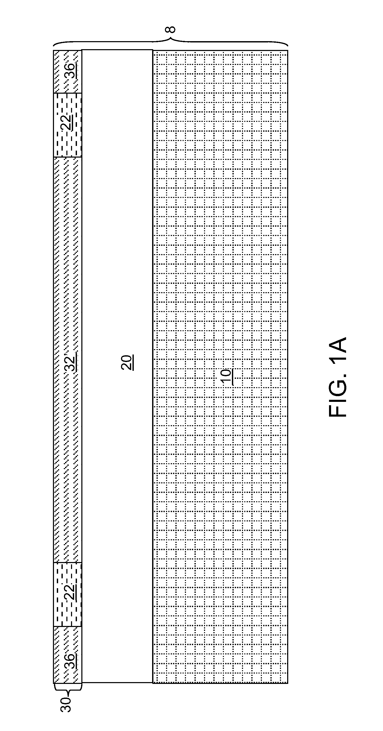
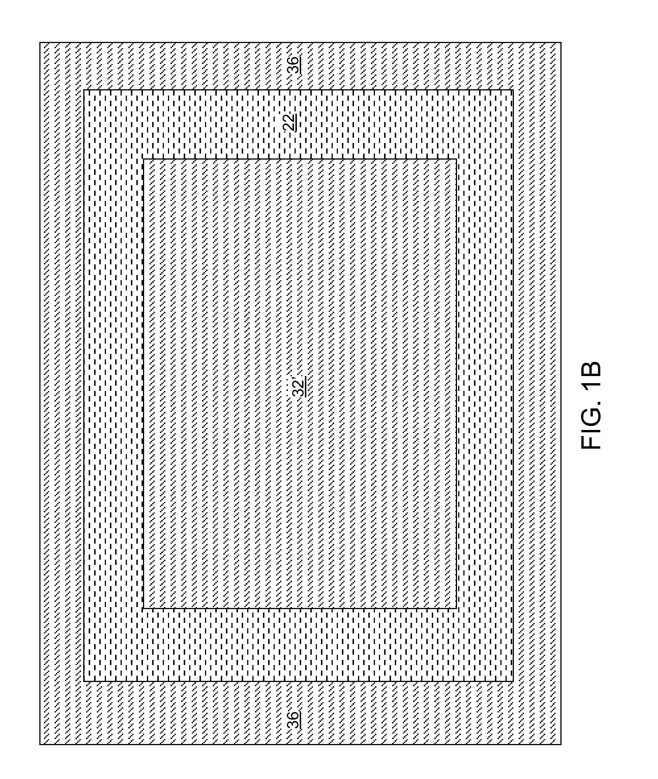
[0025]Referring to FIGS. 1A and 1B, a first exemplary semiconductor structure according to the present disclosure includes a semiconductor-on-insulator (SOI) substrate 8. The SOI substrate 8 includes a stack, from bottom to top, of a handle substrate 10, a buried single crystalline rare earth oxide layer 20, and a top semiconductor layer 30.

[0026]The handle substrate 10 provides structural support to, and prevents deformation or breakage of, the buried single crystalline rare earth oxide layer 20 and the top semiconductor layer 30. The thickness of the handle substrate 10 can be from 50 microns to 2 mm, although lesser and greater thicknesses can also be employed. The handle substrate 10 can include an amorphous, polycrystalline, or single crystalline semiconductor material, an insulator material, a conductor material, or a stack thereof

[0027]The buried single crystalline rare earth oxide layer 20 includes a single crystalline rare earth oxide material. Method of forming a single cr...

second embodiment

[0076]Referring to FIGS. 6A and 6B, a second exemplary semiconductor structure according to the present disclosure can be derived from the first exemplary semiconductor structure of FIGS. 1A and 1B by performing the processing steps of FIGS. 2A and 2B without forming any dummy gate stack (51, 53; See FIGS. 2A and 2B) or any dummy gate spacer (57; See FIGS. 2A and 2B).

[0077]Referring to FIGS. 7A and 7B, the same processing steps are performed as in FIGS. 3A and 3B in the first embodiment with the modification that the edges of the photoresist 77 is laterally shifted to overlie the contiguous single crystalline semiconductor material region 32′.

[0078]Referring to FIGS. 8A and 8B, the processing steps of FIGS. 4A and 4B in the first embodiment are performed. Alternatively, the processing steps for the variation of the first embodiment are performed. A source-side embedded single crystalline semiconductor material region 44 and a drain-side embedded single crystalline semiconductor mate...


PUM


Abstract

After formation of a gate stack, regions in which a source and a drain are to be formed are recessed through the top semiconductor layer and into an upper portion of a buried single crystalline rare earth oxide layer of a semiconductor-on-insulator (SOI) substrate so that a source trench and drain trench are formed. An embedded single crystalline semiconductor portion epitaxially aligned to the buried single crystalline rare earth oxide layer is formed in each of the source trench and the drain trench to form a recessed source and a recessed drain, respectively. Protrusion of the recessed source and recessed drain above the bottom surface of a gate dielectric can be minimized to reduce parasitic capacitive coupling with a gate electrode, while providing low source resistance and drain resistance through the increased thickness of the recessed source and recessed drain relative to the thickness of the top semiconductor layer.

Description

BACKGROUND[0001]The present disclosure relates to semiconductor structures, and particularly to semiconductor structures employing recessed single crystalline source and drain embedded in an upper portion of a buried single crystalline rare earth oxide layer of a semiconductor-on-insulator substrate, and methods of manufacturing the same.[0002]High source resistance or high drain resistance adversely impacts the performance of a field effect transistor by limiting the on-current of the field effect transistor. Thus, devices formed on a semiconductor-on-insulator (SOI) substrate having a thin top semiconductor layer is prone to performance degradation due to reduction in thickness of the source and the drain. For extremely thin semiconductor-on-insulator (ETSOI) devices in which the top semiconductor layer has a thickness less than 30 nm, the problem of high source resistance and high drain resistance significantly degrades the on-current and the overall performance of the ETSOI devi...

Claims


Application Information

Patent Timeline
IPC IPC(8): H01L29/78H01L21/336
CPCH01L21/84H01L29/66477H01L27/1203
Inventor WANG, GENGCHENG, KANGGUOERVIN, JOSEPHPEI, CHENGWENTODI, RAVI M.
Owner GLOBALFOUNDRIES US INC
Why Eureka
Try Eureka