
Fault position analysis method and fault position analysis device for semiconductor device

a fault position analysis and semiconductor technology, applied in the direction of measurement devices, electronic circuit testing, instruments, etc., can solve the problem of inability to specify the position, and achieve the effect of high transmissivity, high quality sic semiconductor devices, and clear detection of the defect position

Active Publication Date: 2013-05-09
FUJI ELECTRIC CO LTD
View PDF5 Cites 12 Cited by
  • Summary
  • Abstract
  • Description
  • Claims
  • Application Information

AI Technical Summary

Benefits of technology

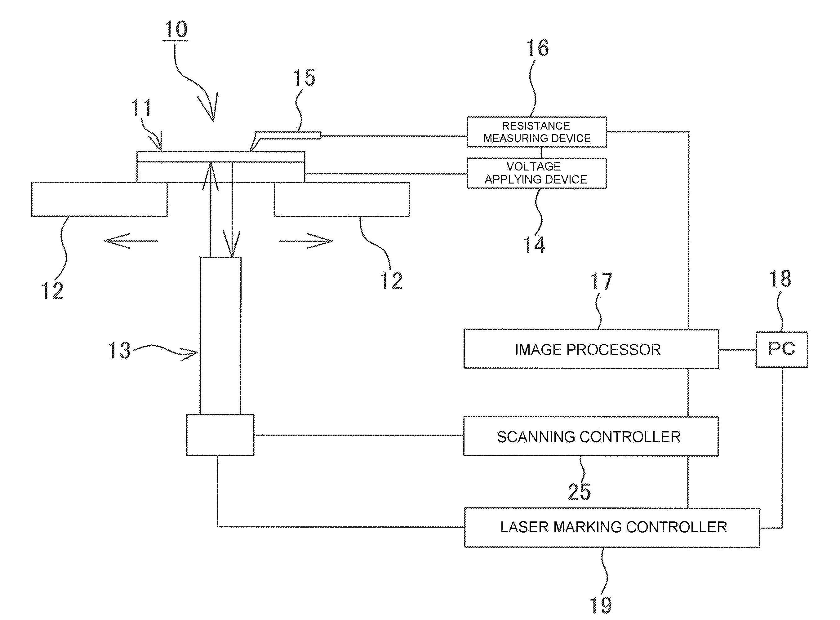
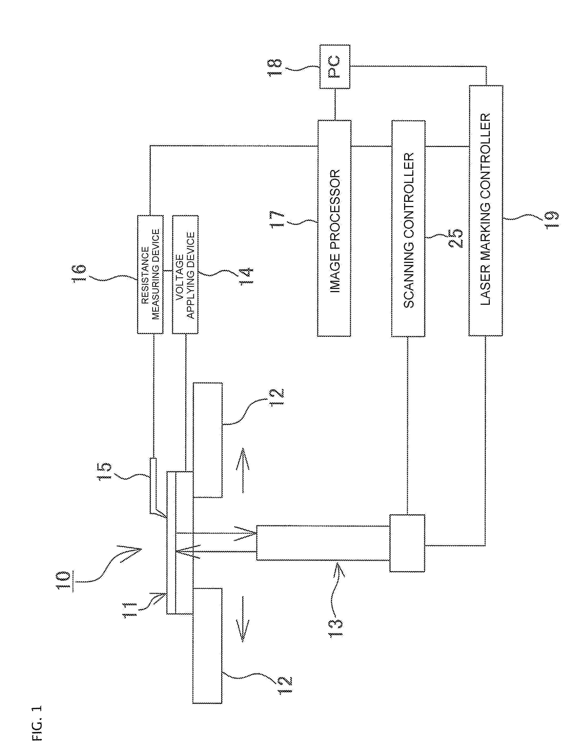
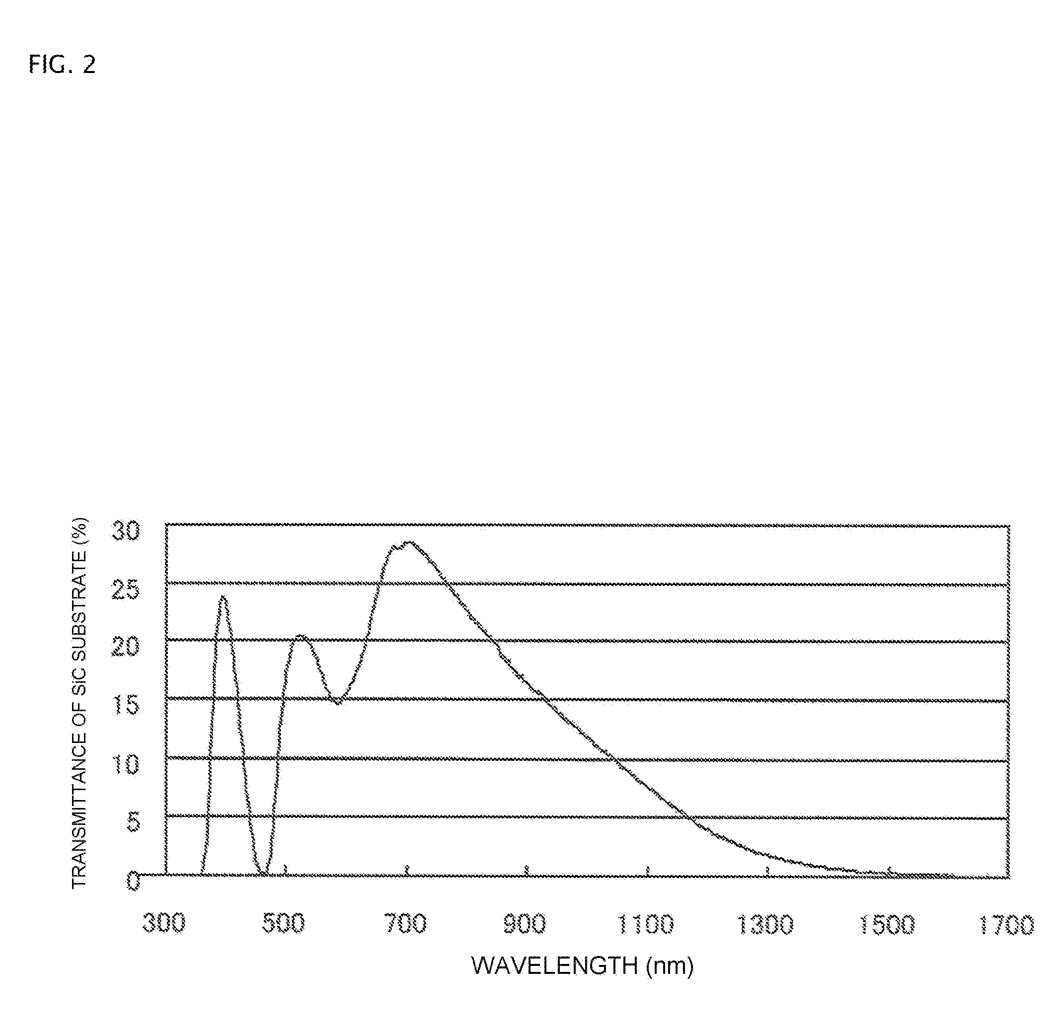
The invention provides a method for analyzing faults in semiconductor devices, particularly those made with N-doped SiC substrates, by using laser beams to irradiate and heat the device and circuit on the front surface of the substrate. The laser beams are able to effectively penetrate the substrate and are shifted away from the band edge of SiC to reduce the chance of carriers exceeding the band gap and causing damage. This method allows for the clear detection of defect positions and the optimization of manufacturing processes for high-quality SiC semiconductor devices.

Problems solved by technology

However, in a case where a sample is a SiC semiconductor device employing the N-doped SiC substrate is electrically defective and thus a leakage current occurs, when measured by a conventional analysis device through the OBIRCH method, a position at which a resistance change occurs is not able to be found, so that it can be seen that the defect position is not able to be specified.

Method used


Image

  • Fault position analysis method and fault position analysis device for semiconductor device
  • Fault position analysis method and fault position analysis device for semiconductor device
  • Fault position analysis method and fault position analysis device for semiconductor device

Examples


example

[0074]Hereinafter, examples of the invention and comparative examples will be described.

examples 1 to 8

, Comparative Examples 1 to 4

[0075]The Schottky barrier diode illustrated in FIG. 3 was manufactured through a typical method. Schottky barrier diode 20 was configured to include N-doped SiC substrate 21, anode electrode (a Schottky electrode) 22 which includes Ti / AI (Ti was formed as a boundary to SiC, and Al was formed as a layer thereon) formed on the front surface of the N-doped SiC substrate, and cathode electrode (an ohmic electrode) 23 which included Ni / Ti / AI (Ni is formed as a boundary to SiC, and Ti and Al are formed as layers thereon) formed on the rear surface. N-doped SiC substrate 21 was configured to include drift layer 21a and cathode layer 21b. The thickness of N-doped SiC substrate 21 was 350 μm.

[0076]In the front surface of the chip of Schottky barrier diode 20, high concentrated P-type ions (1021 atoms / cm3) were implanted to form a φ1 μm pattern, and as illustrated in FIG. 4, the sample having portion 24 as an ohmic contact formed in anode electrode (the Schottky ...


PUM


Abstract

A fault position analysis method and a fault position analysis device for a semiconductor device, through which a fault position of a SiC semiconductor device can be analyzed and specified by an OBI RCH method, are disclosed. The fault position analysis method for the semiconductor device scans and irradiates a device and a circuit on a front surface of a substrate with a laser beam from a rear surface side of the substrate of the semiconductor device to heat the device and the circuit. It causes a current to flow to the device and the circuit while being heated, detects a change in a resistance value caused by a change in a current, and analyzes the fault position. The semiconductor device is a semiconductor device which uses an N-doped SiC substrate. Laser beams having wavelengths of 650 to 810 nm are used.

Description

BACKGROUND OF THE INVENTION[0001]A. Field of the Invention[0002]The present invention relates to a fault position analysis method and a fault position analysis device for a semiconductor device, in which a fault position of the semiconductor device using an N-doped SiC substrate is analyzed by an Optical Beam Induced Resistance Change (OBIRCH) method.[0003]B. Description of the Related Art[0004]Conventionally, the fault positions of a semiconductor device have been specified by a liquid crystal method, an emission microscope, the OBIRCH method, and the like. Among them, the OBIRCH method is an effective method of detecting leakage defects such as disconnections, short circuits, and contact fault, in which the defect portions are irradiated with a laser beam to be locally heated and a resulting change in resistance is detected, thereby specifying the defect position.[0005]As an analysis technique of the OBIRCH method, JP 11-118887 A described below discloses an improved technique in ...

Claims


Application Information

Patent Timeline
Patent Type & Authority Applications(United States)
IPC IPC(8): G01R31/08
CPCG01R31/311
Inventor SUZUKI, KATSUNORIOHI, AKIHIKOKITAMURA, SHOJIOOYAMA, TAKAHIRO
Owner FUJI ELECTRIC CO LTD
Learn More