
Probe block, probe card and probe apparatus both having the probe block

Active Publication Date: 2013-05-09
NIHON MICRONICS
View PDF12 Cites 7 Cited by
  • Summary
  • Abstract
  • Description
  • Claims
  • Application Information

AI Technical Summary

Benefits of technology

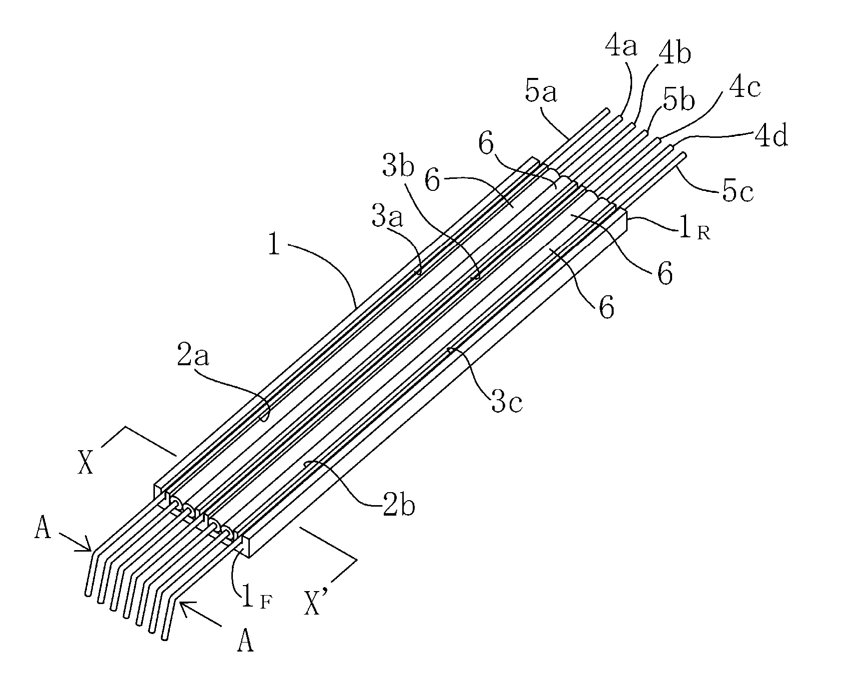
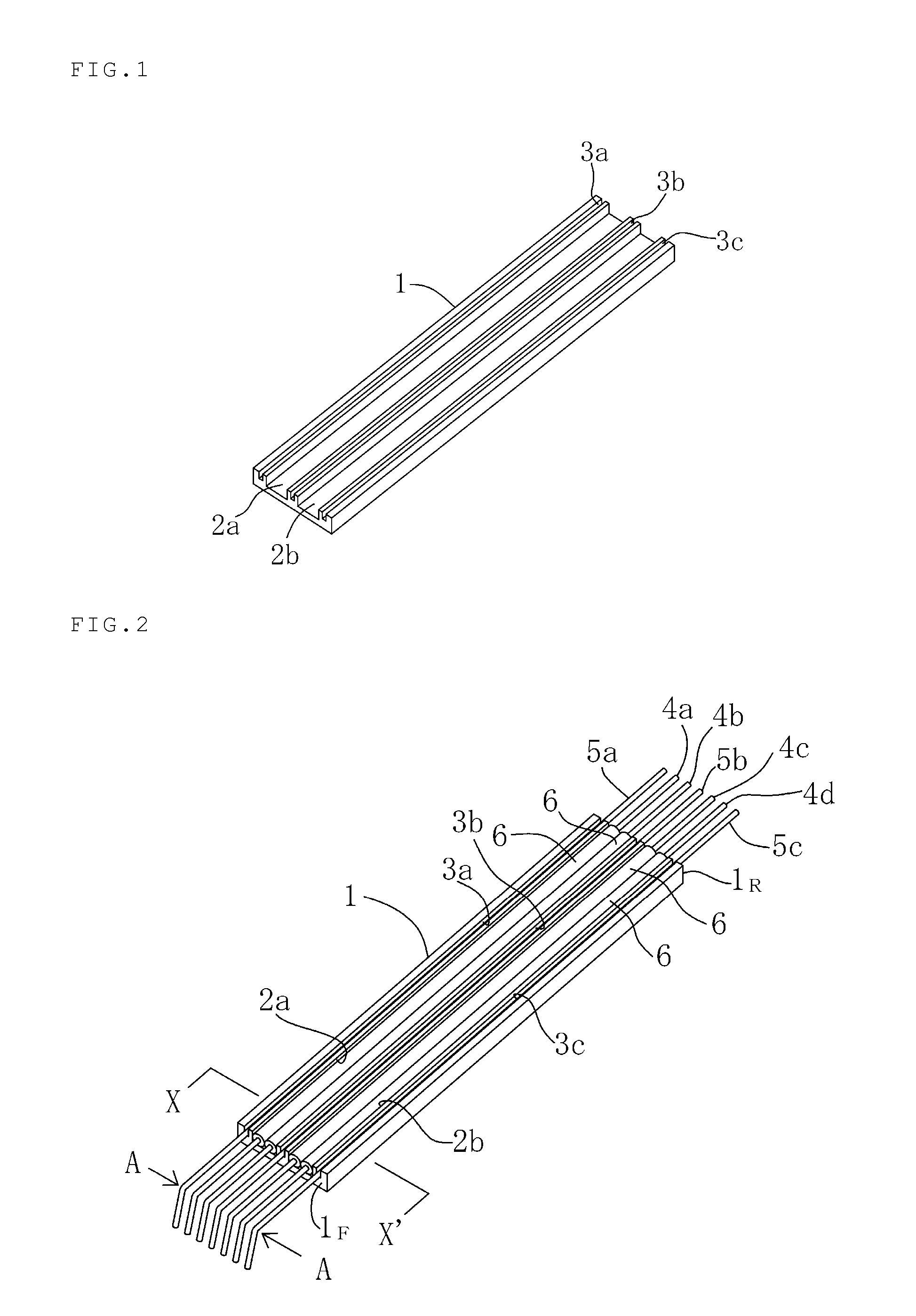
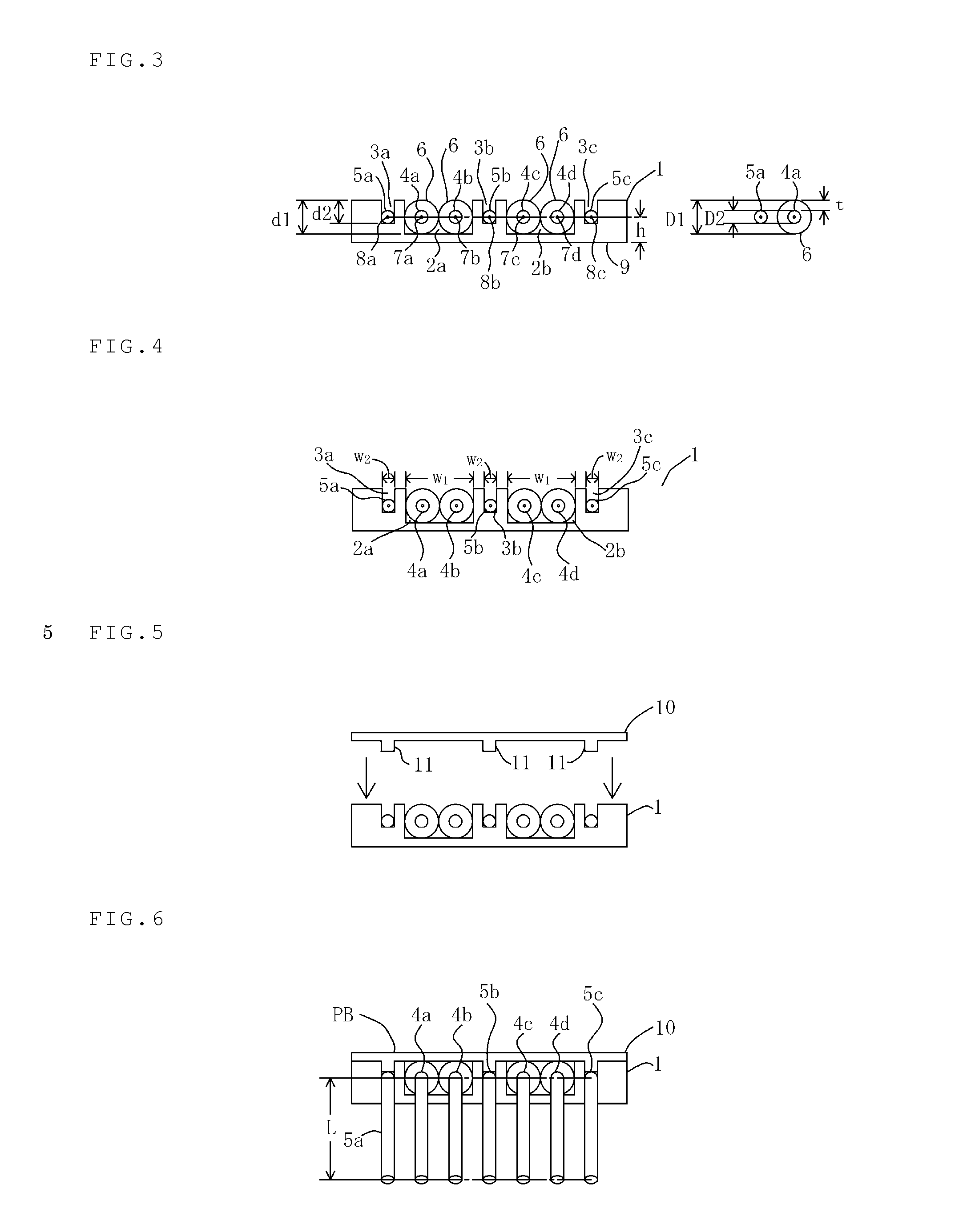
The inventors found a way to create probes that can send balanced signals and are easy to maintain. They did this by placing a pair of probes in a groove on a conductive base. The probes have covers and are placed parallel to each other. These covers make contact with each other, forming a probe block that puts all of them together. This creates a better response at high frequencies and makes maintenance easier.

Problems solved by technology

Therefore, the probe card has disadvantages that each of the probe needles is not so flexible enough to contact sufficiently with a bonding pad of semiconductor device under test.
In addition, it is not so easy to assemble the probe card, because more than one probe needles have to be collected and fixed with conductive substance.
On the same reasons, the maintenance of the probe card, such as exchange of probe needles, is difficult.
However, the probe card employs parallel two-wire lines structure in tip portion of the probes, because it is hard to employ coaxial structure there.
For this reason, it is not easy to assemble the probe card.
In addition, satisfying high-frequency response characteristics are not achieved in the probe card, because the ground probe is different from the signal transmitting probes in its height and in its length.
Because of this, there are disadvantages in the probe card that installation and removal of the probes are not so easy.
Therefore, it is difficult to keep constant the space between two probe needles which form balanced transmission line, and consequently there are drawbacks in the probe card that noise is not decreased sufficiently.

Method used


Image

  • Probe block, probe card and probe apparatus both having the probe block
  • Probe block, probe card and probe apparatus both having the probe block
  • Probe block, probe card and probe apparatus both having the probe block

Examples


example 1

[0065]A probe block having a conformation represented by “GSSGSSG” and probe pitch of 110 μm was prepared using the following materials, and its transmission characteristics were measured and compared with those of the following conventional coaxial cable.

[0066]Probe material: tungsten-base alloy (diameter is 0.038 mm)

[0067]Probe length: 25 mm

[0068]Length of the front portion: 1.0 mm

[0069]Dielectric cover: fluororesin (outside diameter is 0.11 mm)

[0070]Probe material: tungsten-base alloy (diameter is 0.038 mm)

[0071]Probe length: 25 mm

[0072]Length of the front portion: 1.0 mm

[0073]Probe material: tungsten-base alloy (diameter is 0.13 mm)

[0074]Probe length: 25 mm

[0075]Length of the front portion: 3.2 to 3.7 mm

[0076]Dielectric cover: fluororesin (outside diameter is 0.42 mm)

[0077]Insertion loss (S21) was measured using the following measuring apparatus and in accordance with the following procedures.

[0078]Measuring apparatus: Network Analyzer (produced by Agilent Technologies, U.S.A. T...


PUM


Abstract

The present invention provides a probe block, which comprises 1) a conductive base on which a first groove is formed, 2) a pair of signal transmitting probes which have dielectric covers and are placed parallel to each other in the first groove, and 3) a ground probe which is in contact with the conductive base, wherein front portions of the signal transmitting probes and the ground probe protrude from the conductive base to form signal transmitting probe needles and a ground probe needle, respectively. The probe block of the present invention has excellent high frequency responses characteristics and is easy for maintenance.

Description

BACKGROUND OF THE INVENTION[0001]1. Field of the Invention[0002]The present invention relates to a probe block, in particular a probe block suitable for transmitting balanced signal, and a probe card and a probe apparatus both having said probe block.[0003]2. Description of the Related Art[0004]In recent years, with improvements in performance of semiconductor devices, it is desired to improve frequency response characteristics of inspecting apparatus which inspects electrical properties of semiconductor devices. Japanese Patent No. 2765247, for example, discloses a probe card, in which at least one probe needle is covered with dielectric film except its tip portion, and the surface of the dielectric film and conductive surfaces of other probe needles are covered with conductive substance to electrically connect them, thereby decreasing parasitic capacitance between probe needles and improving isolation between probe needles. In the probe card, however, since the probe needles are c...

Claims


Application Information

Patent Timeline
IPC IPC(8): G01R1/067
CPCG01R1/06772G01R1/073H01L22/00
Inventor OGASAWARA, TAKASHIYAMAGUCHI, NORIE
Owner NIHON MICRONICS
Learn More