

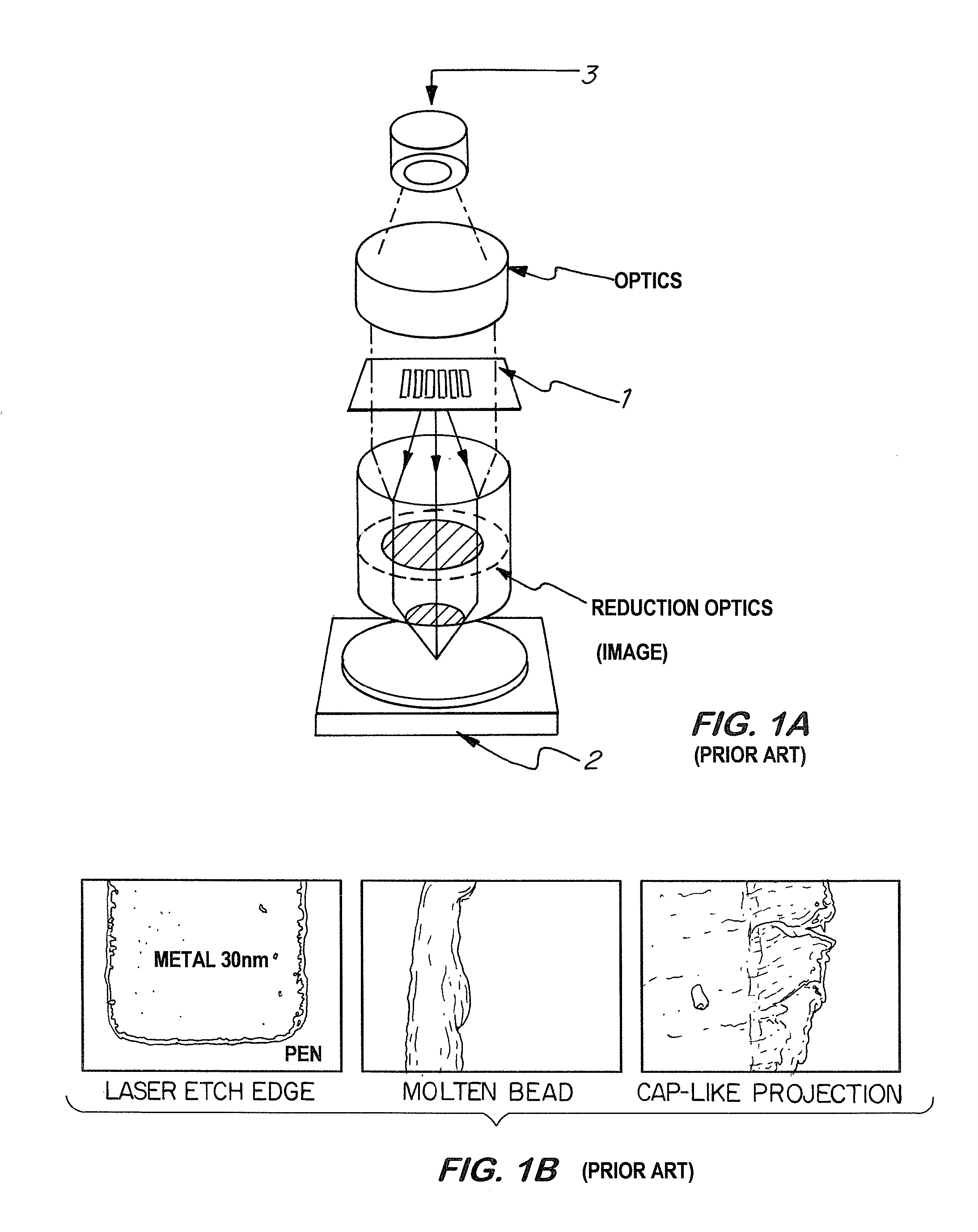
Reduction of the effects of cap-like projections, due to laser ablation of a metal level by using a non-crosslinked light or heat-crosslinkable polymer layer
a technology of laser ablation and polymer layer, which is applied in the manufacture of resistors, capacitors, diodes, etc., can solve the problems of step crossing difficulties, premature aging, and electric leakage, and achieve the effect of reducing the appearance of cap-like projections
- Summary
- Abstract
- Description
- Claims
- Application Information
AI Technical Summary
Benefits of technology
Problems solved by technology
Method used
Image

Examples
Embodiment Construction
[0097]1 / High-Gate Architecture:
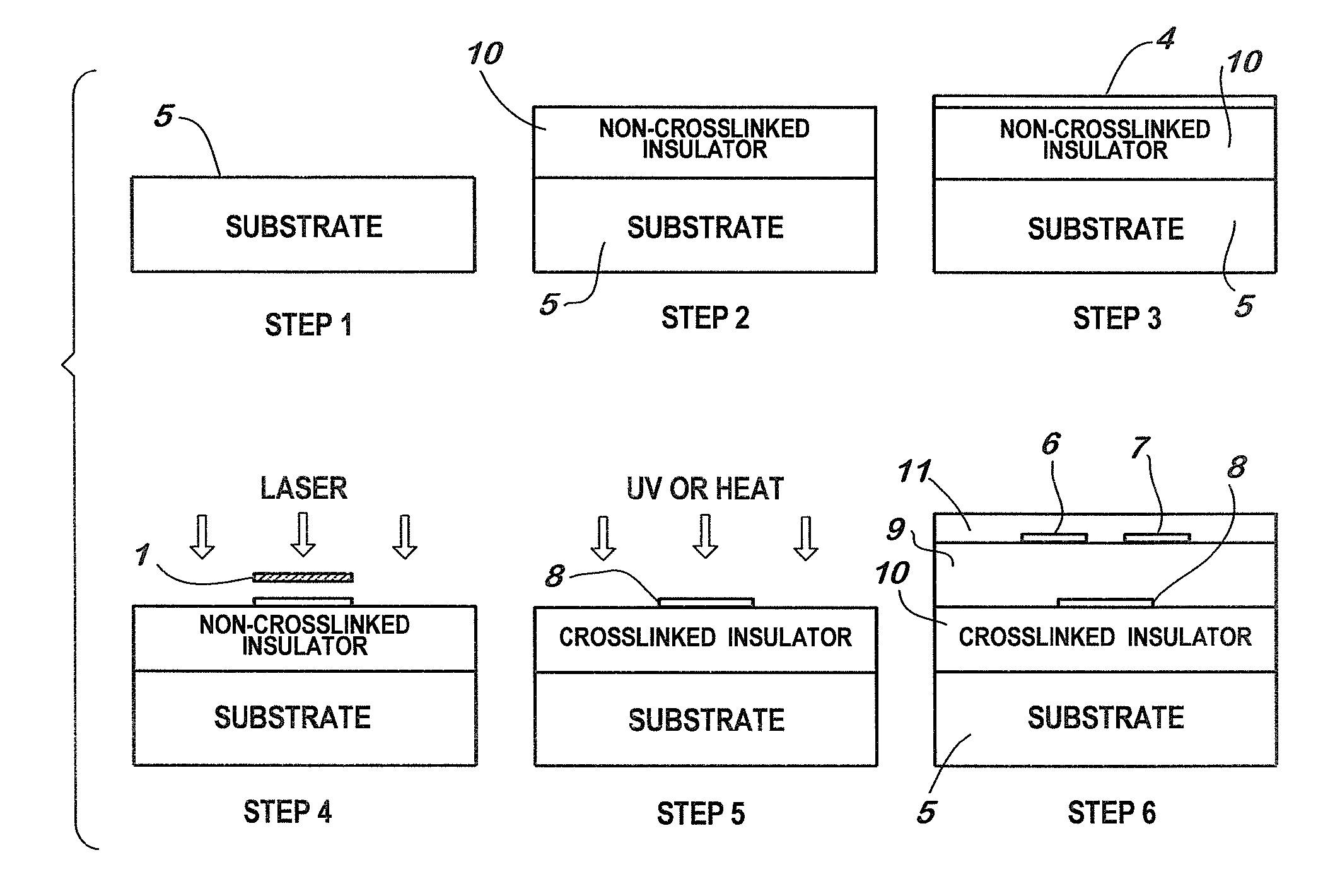
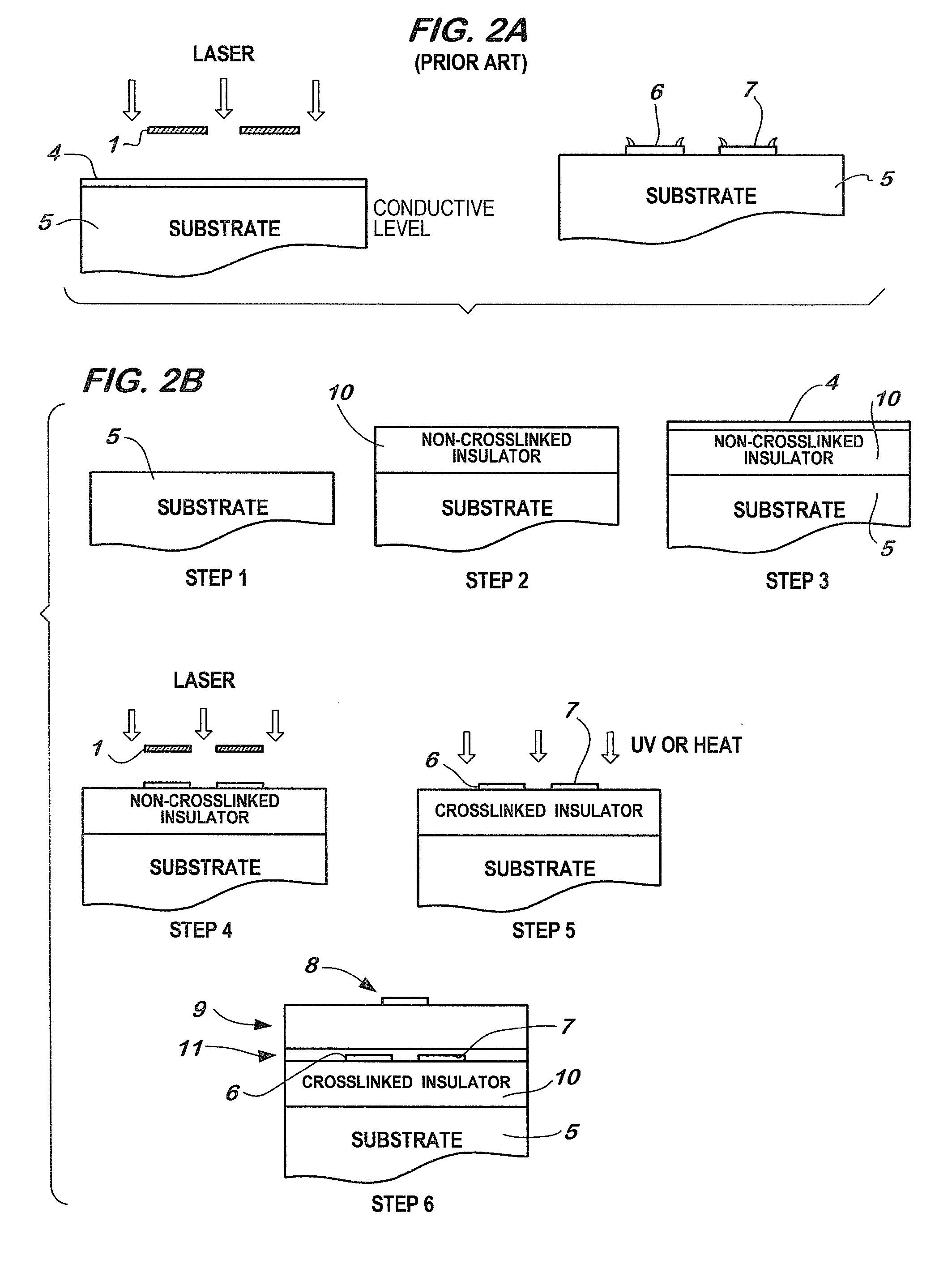
[0098]The implementation of the present invention in the context of a high-gate architecture is illustrated in FIG. 2B. It is mainly based on the deposition of a non-crosslinked or partially crosslinked insulating polymer (10), which is thus crosslinkable, between the substrate (5) and the conductive level (4).
[0099]a / Insulating Crosslinkable Polymer:
[0100]The insulating crosslinkable polymer, capable of being used in high-gate architecture, may be selected from the following list:
[0101]polyacrylates;
[0102]epoxy resins;
[0103]epoxy acrylates;
[0104]polyurethanes;
[0105]silicons.
[0106]In this architecture, the insulator (10) enables, if it is non-crosslinked or partially crosslinked, to decrease cap-like projections in the step of ablation of the upper layer (4). It must be electrically insulating to avoid disturbing the semiconductor layer (11) deposited above.
[0107]b / Method for Manufacturing the High-Gate Architecture:[0108]Step 1: substrate (5)[0109]...
PUM
 Abstract
Description
Claims
Application Information