
Reduction of the effects of cap-like projections, due to laser ablation of a metal level by using a non-crosslinked light or heat-crosslinkable polymer layer

a technology of laser ablation and polymer layer, which is applied in the manufacture of resistors, capacitors, diodes, etc., can solve the problems of step crossing difficulties, premature aging, and electric leakage, and achieve the effect of reducing the appearance of cap-like projections

Inactive Publication Date: 2013-11-12
COMMISSARIAT A LENERGIE ATOMIQUE ET AUX ENERGIES ALTERNATIVES
View PDF4 Cites 0 Cited by
  • Summary
  • Abstract
  • Description
  • Claims
  • Application Information

AI Technical Summary

Benefits of technology

The present invention relates to a method for reducing defects in a laser-processed metal layer, such as cap-like projections and molten edges, by using a crosslinkable material placed under the metal layer. The crosslinkable material absorbs some of the laser power, resulting in less damage to the metal layer and improved electrical characteristics. The crosslinkable material can be in a non-crosslinked or partially crosslinked form, with the degree of crosslinking affecting its properties. The crosslinkable material can be made from a laser-crosslinkable material that is not fully crosslinked, allowing for a balance of hardness and resiliency. Overall, the invention reduces defects and improves the quality of laser-processed metal layers.

Problems solved by technology

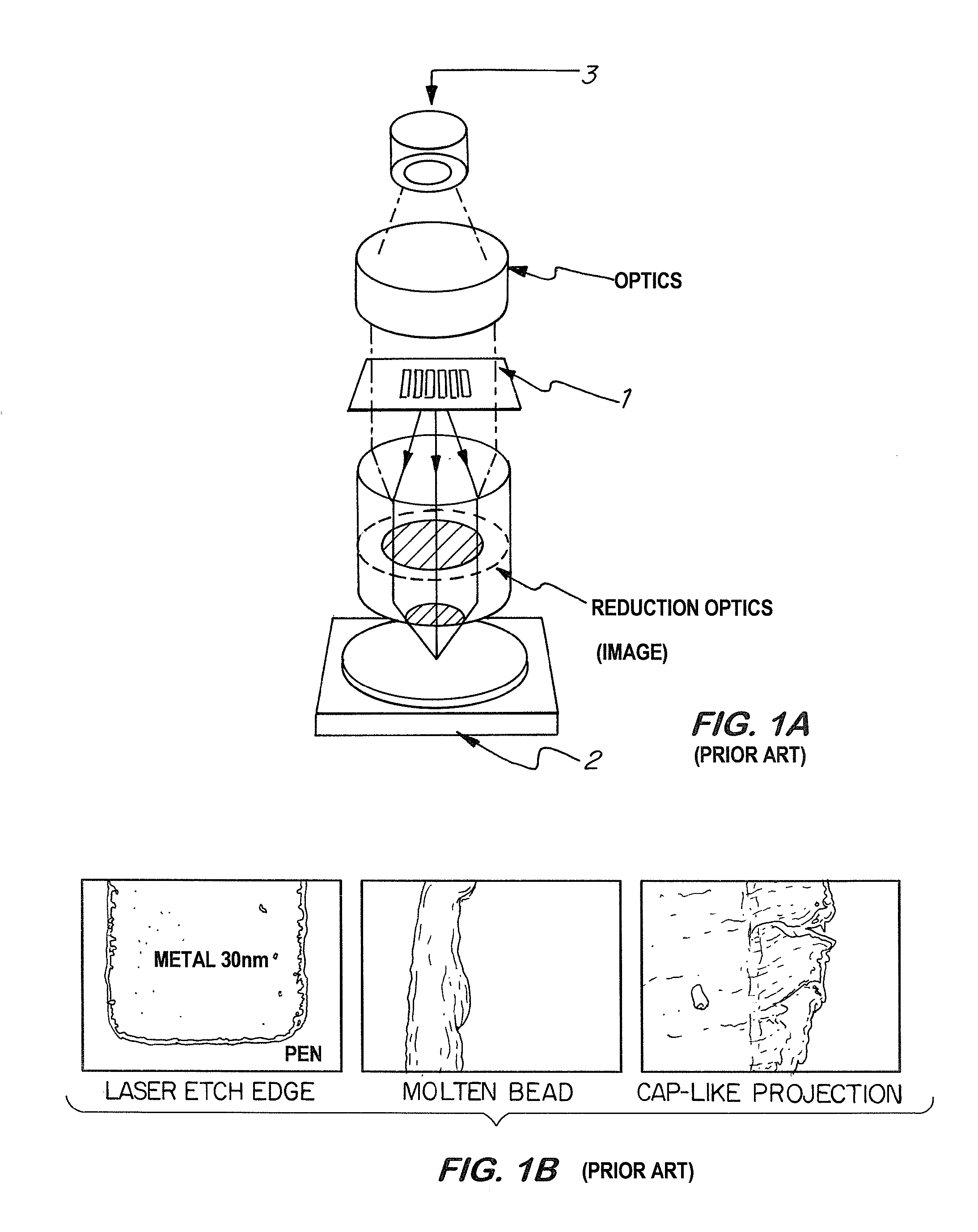
Such profiles are a great issue for the use of these patterns in the forming of organic electronic components, for which techniques of deposition of active layers having a thickness on the order of 100 nanometers are used.
Depositing thin layers of 100 nanometers or less, for example semiconductors from 30 to 70 nanometers on patterns exhibiting such projections and profiles raises many issues.
This may especially cause electric leakages, step crossing difficulties, dimension losses (for example, concerning the channel width), a premature aging .
This disadvantage is a major concern in microelectronics, and especially in the forming of transistors.
However, the stacking of different organic and / or inorganic layers raises a number of issues.

Method used


Image

  • Reduction of the effects of cap-like projections, due to laser ablation of a metal level by using a non-crosslinked light or heat-crosslinkable polymer layer
  • Reduction of the effects of cap-like projections, due to laser ablation of a metal level by using a non-crosslinked light or heat-crosslinkable polymer layer
  • Reduction of the effects of cap-like projections, due to laser ablation of a metal level by using a non-crosslinked light or heat-crosslinkable polymer layer

Examples


Embodiment Construction

[0097]1 / High-Gate Architecture:

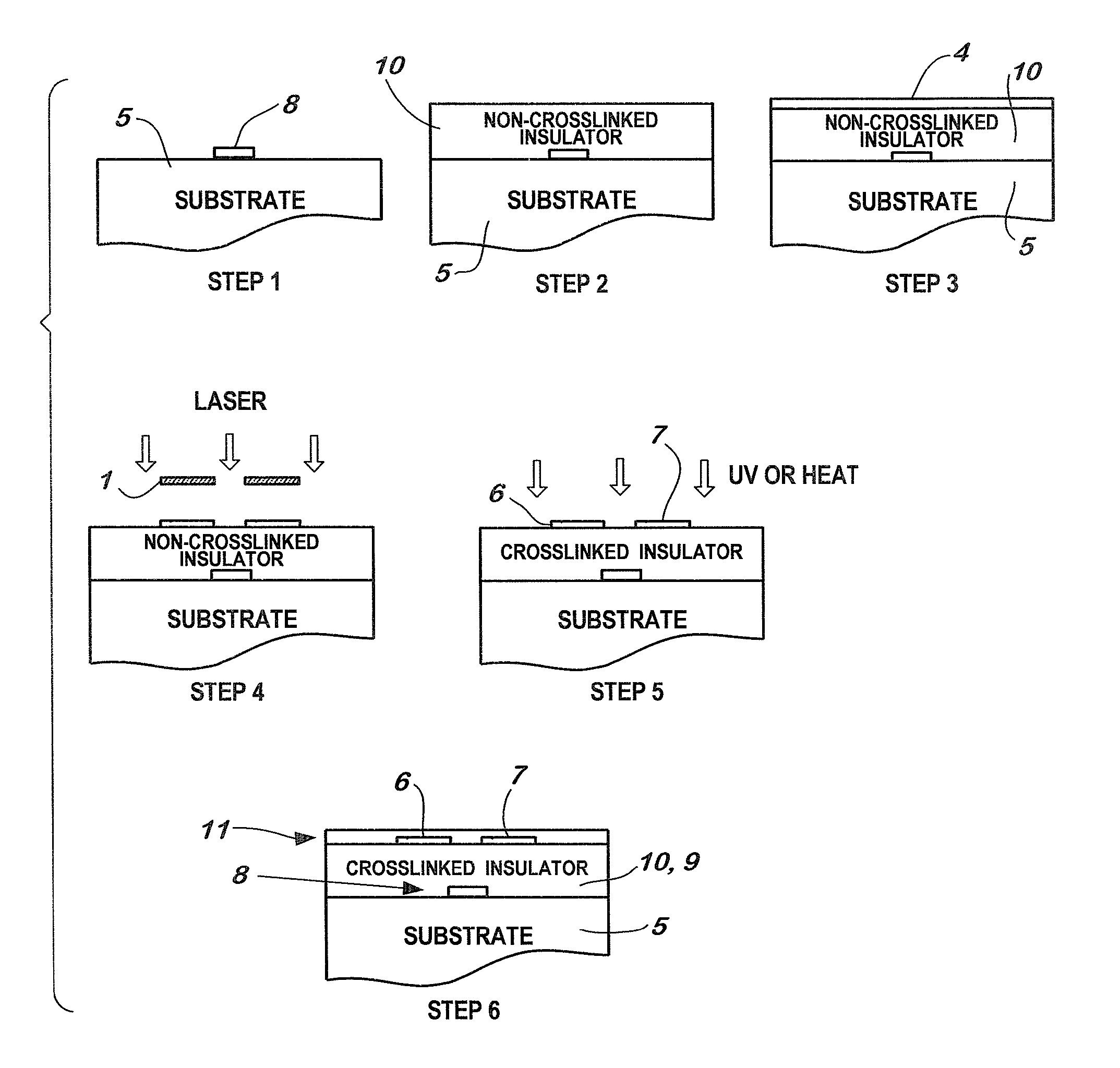
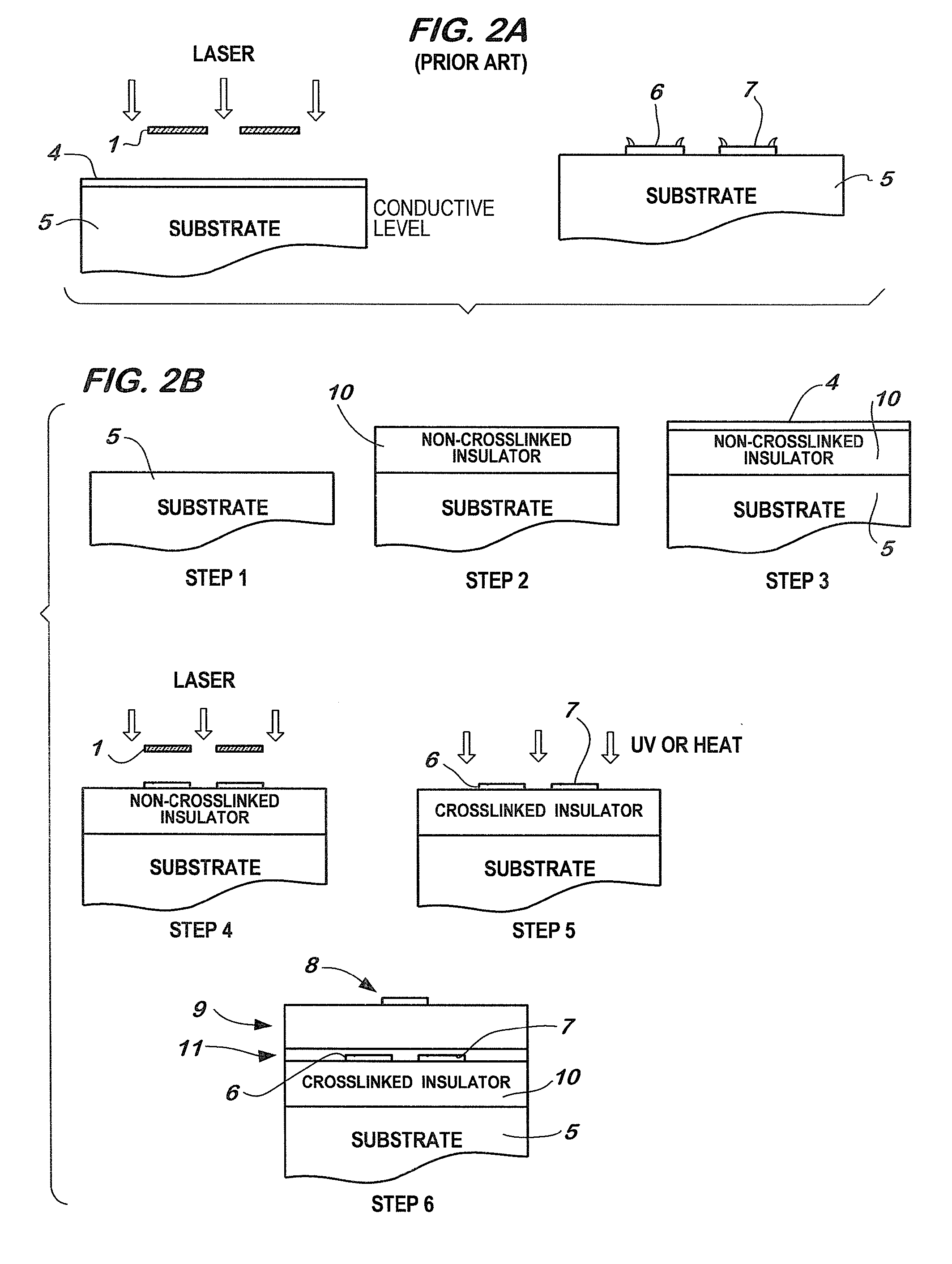
[0098]The implementation of the present invention in the context of a high-gate architecture is illustrated in FIG. 2B. It is mainly based on the deposition of a non-crosslinked or partially crosslinked insulating polymer (10), which is thus crosslinkable, between the substrate (5) and the conductive level (4).

[0099]a / Insulating Crosslinkable Polymer:

[0100]The insulating crosslinkable polymer, capable of being used in high-gate architecture, may be selected from the following list:

[0101]polyacrylates;

[0102]epoxy resins;

[0103]epoxy acrylates;

[0104]polyurethanes;

[0105]silicons.

[0106]In this architecture, the insulator (10) enables, if it is non-crosslinked or partially crosslinked, to decrease cap-like projections in the step of ablation of the upper layer (4). It must be electrically insulating to avoid disturbing the semiconductor layer (11) deposited above.

[0107]b / Method for Manufacturing the High-Gate Architecture:[0108]Step 1: substrate (5)[0109]Ste...


PUM


Abstract

A laser-crosslinkable material appearing in non-crosslinked or partially crosslinked form is used to protect, during a laser etching, the electrodes of an organic transistor.

Description

FIELD OF THE INVENTION[0001]The present disclosure relates to the field of organic electronics, and especially to the manufacturing of resistors, capacitors, diodes, transistors . . . .[0002]In practice, it provides a solution to issues related to surface degradation in step(s) of etching of a metal level. It finds a more specific application in the step of etching by excimer-type laser ablation of the electrodes of an organic transistor.BACKGROUND OF THE INVENTION[0003]The excimer method, which may be implemented by means of a device illustrated in FIG. 1A, enables to structure and to pattern patterns obtained by the projection of a mask (1). The ablation of the substrate (2) is achieved by the interaction between the UV beam (3, excimer) crossing the mask (1) made of glass and aluminum and the layer surface (substrate, 2).[0004]The excimer laser is a gas laser which emits in pulsed mode in the ultraviolet range, between 193 and 351 nanometers according to the gas mixture used. The...

Claims


Application Information

Patent Timeline
Patent Type & Authority Patents(United States)
IPC IPC(8): H01L51/40H10K99/00
CPCH01L51/0023H01L51/052H01L51/0512H01L51/0541H01L51/0545H10K71/621H10K10/471H10K10/464H10K10/466H10K10/00H10K10/462
Inventor HEITZMANN, MARIEBENWADIH, MOHAMMED
Owner COMMISSARIAT A LENERGIE ATOMIQUE ET AUX ENERGIES ALTERNATIVES
Learn More